Service Manuals, User Guides, Schematic Diagrams or docs for : Pioneer DVD pioneer cd IC_pdf MN677532JAUB
<< Back | HomeMost service manuals and schematics are PDF files, so You will need Adobre Acrobat Reader to view : Acrobat Download Some of the files are DjVu format. Readers and resources available here : DjVu Resources
For the compressed files, most common are zip and rar. Please, extract files with Your favorite compression software ( WinZip, WinRAR ... ) before viewing. If a document has multiple parts, You should download all, before extracting.
Good luck. Repair on Your own risk. Make sure You know what You are doing.
Image preview - the first page of the document
>> Download MN677532JAUB documenatation <<
Text preview - extract from the document
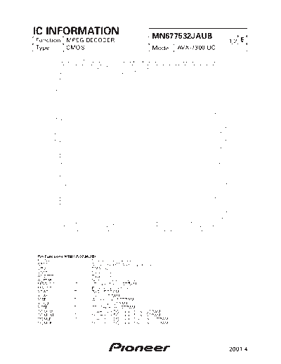
IC INFORMATION                                       MN677532JAUB
Function MPEG DECODER                                                         1/2 E
Type     CMOS                                        Model      AVX-7300/UC


Pin Functions(MN677532JAUB)
Pin Name         I/O     Function and Operation
STD7-0             I     Stream data/CD-Audio bypass port
VRQ               O      DMA request
VSTR               I     Data strobe
AUDSTR             I     Data strobe
AVRTM              I     Sector separation signal
MDQ15-0          I/O     I/O data of main SDRAM
MA11-0            O      Bank sell and address
XRAS              O      RAS ofSDRAM
XCAS              O      CAS of SDRAM
XWE               O      Write signal of SDRAM
XCSM              O      CS of main SDRAM
XCSE              O      CS of extended SDRAM
DQMLM             O      Lower byte DQ mask of main SDRAM
DQMUM             O      Upper byte DQ mask of main SDRAM
DQMLE             O      Lower byte DQ mask of extended SDRAM
DQMUE             O      Upper byte DQ mask of extended SDRAM


                                                                              2001.4
IC INFORMATION                                            MN677532JAUB
Function MPEG DECODER                                                                2/2 E
Type     CMOS                                             Model        AVX-7300/UC
Pin Functions(MN677532JAUB)
Pin Name         I/O     Function and Operation
MCK               O      SDRAM CLK
MCKI               I     SDRAM CLK input
HD15-0           I/O     Data bus
HA11-1             I     Address bus
HCLK               I     Host CPU clock
XCS                I     Chip select
XRD                I     Read enable
XWR                I     Write enable
XDK               O      Data acknowledge
XHINT             O      Interrupt strobe
HMD0,1             I     Host CPU select
XRST               I     System reset
CLK27              I     27MHz clock input
CLKMON            O      Clock monitor
CKIO               I     81MHz clock select
ACKIO              I     Audio PLL test mode
CLK81              I     External 81MHz input
CLK121             I     External 121.5MHz input
MODE121            I     Clock mode select
DCTEST             I     DC test mode
TESTSEL1,0        O      Test signal
TEST10-0          O      Test signal
VD7-0             O      Video data bus
VCLK              O      Video data clock
XVSYNCO          I/O     Vsync input/output
XHSYNCO          I/O     Horizontal sync input/output
VYOUT             O      Y analog output
VCOUT             O      Cr C analog output
VGOUT             O      Cb Composite analog output
VBOUT             O      C analog output
VREFY/C/G/B        I     DAC reference input
IREFY/C/G/B        I     DAC resistance terminal for bias current setting
COMPY/C/G/B        I     DAC capacity connection terminal for stabilization
RFF               O      Repeat first field flag output
ADOUT2-0          O      Audio data output
SRCK              O      Bit clock output
LRCK              O      LR clock output
DACCK             O      DAC clock output
IECOUT            O      IEC958 data output
TCPOUT            O      OPEN
ATCPOUT           O      OPEN
ATVROUT           O      L fixation
EXTCK              I     External audio clock input
VSS                      GND
VDD                      Power supply
LVDD                     Lch Power supply
PLLAVDD                  PLL analog power supply
PLLVDD                   PLL power supply
PLLAVSS                  PLL analog GND
APLLVDD                  Analog PLL power supply
AVDD                     Analog power supply
AVSS                     Analog GND
APLLAVDD                 Analog PLL power supply for audio
APLLAVSS                 Analog PLL GND for audio


                                                                                     2001.4
◦ Jabse Service Manual Search 2026 ◦ Jabse Pravopis ◦ onTap.bg ◦ Other service manual resources online : Fixya ◦ eServiceinfo