Service Manuals, User Guides, Schematic Diagrams or docs for : Pioneer DVD pioneer cd IC_pdf TA2153FN
<< Back | HomeMost service manuals and schematics are PDF files, so You will need Adobre Acrobat Reader to view : Acrobat Download Some of the files are DjVu format. Readers and resources available here : DjVu Resources
For the compressed files, most common are zip and rar. Please, extract files with Your favorite compression software ( WinZip, WinRAR ... ) before viewing. If a document has multiple parts, You should download all, before extracting.
Good luck. Repair on Your own risk. Make sure You know what You are doing.
Image preview - the first page of the document
>> Download TA2153FN documenatation <<
Text preview - extract from the document
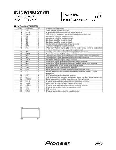
IC INFORMATION                                          TA2153FN
Function RF AMP                                                                     1/1 E
Type     Bipolar                                        Model        DEH-P630/X1N/UC

- Pin Functions(TA2153FN)
  Pin No.   Pin Name        I/O   Function and Operation
        1   VCC             -     Power supply voltage terminal
        2   RFGC            I     RF amplitude adjustment control signal terminal
        3   GMAD            I     AGC amplifier frequency characteristic adjustment terminal
        4   FNI             I     Main beam amplifier input terminal
        5   FPI             I     Main beam amplifier input terminal
        6   TPI             I     Sub beam amplifier input terminal
        7   TNI             I     Sub beam amplifier input terminal
        8   MDI             O     Monitor photodiode amplifier input terminal
        9   LDO             I     Laser diode amplifier output terminal
       10   SEL             I     APC circuit ON/OFF signal, LDO terminal control input terminal and bottom
                                  and peak detection frequency switching terminals
      11    TEB             I     Tracking error balance adjustment signal input terminal
      12    2VRO            O     Reference voltage (2VRO) output terminal
      13    TEN             I     Tracking error signal generation amplifier reverse phase input terminal
      14    TEO             O     Tracking error signal generation amplifier output terminal
      15    SBAD            O     Sub beam addition signal output terminal
      16    FEO             O     Focus error signal generation amplifier output terminal
      17    FEN             I     Focus error signal generation amplifier reverse phase input terminal
      18    SEB             I     RFRP generation circuit mode switching terminal
      19    VRO             O     Reference voltage (VREF) output terminal
      20    RFRP            O     Signal generation amplifier output terminal for track count
      21    BTC             I     Bottom detection time constant adjustment terminal for RFCT signal
                                  generation
      22    RFCT            O     RFRP signal center level output terminal
      23    PKC             I     Peak detection time constant adjustment signal for RFCT signal generation
      24    RFRPIN          I     Signal generation amplifier input terminal for track count
      25    RFGO            O     RF signal amplitude adjustment amplifier output terminal
      26    GVSW            I     AGC, FE or TE amplifier gain switching terminal
      27    AGCIN           I     RF signal amplitude adjustment amplifier input terminal
      28    RFO             O     RF signal generation amplifier output terminal
      29    GND             I     GND terminal
      30    RFN2            I     RF signal generation amplifier input terminal


      15                1


      16               30


                                                                                                 2001.2
◦ Jabse Service Manual Search 2026 ◦ Jabse Pravopis ◦ onTap.bg ◦ Other service manual resources online : Fixya ◦ eServiceinfo