Service Manuals, User Guides, Schematic Diagrams or docs for : Quanta Quanta_A03

<< Back | Home

Most service manuals and schematics are PDF files, so You will need Adobre Acrobat Reader to view : Acrobat Download Some of the files are DjVu format. Readers and resources available here : DjVu Resources
For the compressed files, most common are zip and rar. Please, extract files with Your favorite compression software ( WinZip, WinRAR ... ) before viewing. If a document has multiple parts, You should download all, before extracting.
Good luck. Repair on Your own risk. Make sure You know what You are doing.


Image preview - the first page of the document
Quanta_A03


>> Download Quanta_A03 documenatation <<

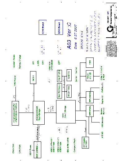
Text preview - extract from the document
                  5                             4                                         3                                                    2                                                                           1


        Clock Gen
                                       P4 M/Celeron M CPU             VID[0:5]                              System Power
                                                                                    CPU Power
                                       479P FCBGA/FCPGA
D       CPU FAN                                                                                            Battery Charge                                                                                                                                D


                                                    FSB
                                                    400MHz
      DDR Power
                                                                             DVO          SiI164                DVI

    DDR SODIMM x 1    DDR Interface     852GM/855GME
                                                                                                                LVDS
                      200/266/333MHz    North Bridge
                                                                                                                             VGA/USB/DIO/I2C
                                                                                                                CRT                                                                          EZAD Board
                                                                                                                             5M Cable
C                                                                                                                                                                                                                                                        C
                                                    HUB
                                                                                     USB 2.0              USB HUB
         USB 2.0 Port 0/1                           Interface
                                                                                                          CY7C65630
         USB A type                                 66MHz

         USB 2.0 Port 2/3                                                                                                    VGA/USB/DIO/I2C
                            USB 2.0                                     MiniPCI Slot x1   XGI Z7 GPU            CRT                                                                          EZAD Board
         USB A type                                                                                                          5M Cable
                                           ICH4                                    PCI 33MHZ
                                           South Bridge

                                                                                                                                                   A03 Ver :C
                            ATA100
         IDE 40PIN/44PIN
                                                                         RTL8110SC             SiI3512E


B
         Compact Flash
                                                                                          SATA1      SATA2                                         Date : 6/27/2007                                                                                      B


                                                                 LPC 33MHz
                                                                                                                                                   852GM/ ICH4
              A97 Codec      AC97
              ALC655
                                                                                               Fintek                                  PCB P/N: DA0A03MB8C0
                                              WPC8763L            WPCN383U                     81218D           FWH
                                                                                                                                       DIP P/N : 31A03MB0000/10/20/30
                                                                                                                                       CS SMT P/N : 41A03CS0000/10/20/30
                                                                                                                                       SS SMT P/N : 51A03SS0000/10/20/30
                                              Battery                                         COM 1/2/3/4/5/6
A                        KB/MS   HW Monitor                     Digital IO     PARALLEL                                                                                                                                                                  A
                                              Monitor                                         & IrDA
                                                                                                                                         PROPRIETARY NOTE
                                                                                                                       The content of this technical information (the Data) has
                                                                                                                        been originated by or is peculiarly within the knowledge
                                                                                                                       of Quanta Computer INC. Tao Yuan, Taiwan. This Data
                                                                                                                                                                                                                      PROJECT: A03
                                                                                                                        is the property of Quanta Computer INC. and is subject
                                                                                                                       to protection under recognized legal principles. The Data
                                                                                                                       should be used or disclosed for limited purposes as defined
                                                                                                                       in the corresponding agreement. This Data may not be
                                                                                                                                                                                                                     Quanta Computer Inc.
                                                                                                                       transferred from the custody of Quanta Computer INC.,
                                                                                                                       except as authorized by Quanta Computer INC and may           Size    Document Number                                     Rev
                                                                                                                       not be used by or disclosed to person neither having            A3                                                     C1A
                                                                                                                       confidential obligations nor having a need for such use or
                                                                                                                       disclosure consistent with the purpose without the prior
                                                                                                                                                                                                            Black Diagram
                                                                                                                       written consent of Quanta Computer INC.
                                                                                                                                                                                     Date:   Friday, June 29, 2007         Sheet   1   of   38
                  5                             4                                         3                                                      2                                                                         1
                       5                                                                     4                          3                                                  2                                                                                                         1


                                                                                                                                  PWR_ON_EC
                                                                                                                                                        PWR_ON_12V
                                                                                                                                  SLP_S3_N                                                                                                        P5V                        IMVP-IV                    P_VCORE
                                                                                                                                                                                                                                                                             MAX1907


                                                                                                                                              +5V_STBY&
                                                                                                  Power Jack                VIN                            P5V_STBY                             P5V
D                                                                                                                                             +3.3V_STBY               +5V Rrgulator                                                       +1.5V Rrgulator                          P_1V5                                         D
                                                                                                  +19V Input
                                                                                                                                              PWM TPS51120             FDS6294                                                             G5626


                                                                                                                                                           P3V3_STBY                            P3V3
                                                                                                                                                                       +3.3V Rrgulator
                                                                                                                                                                       FDS6294
                                                                                                                Battery Charger
                                                                                                 Battery Cell
                                                                                                                MAX8726                                                                                                   PG_3_5_12_OK
                                                                                                                                                             VIN                                P12V
                                                                                                                                                                         +12V PWM
                                                                                                                                                                                                                                                                                    V1_05_PWROK
                                                                                                                                                                         ISL6545

                                                                                                                                                                               PG_3_5_12_OK_N


                                                                                                                                                              VIN       +2.5V&P_VMCH                                         P_VMCH                                                                     P1V05
                                                                                                                                                                                                                                                                      +1.05V Rrgulator
                                                                                                                                                                        PWM TPS51120
                                                                                                                                                                                                                                                                      SC338

C                                                                                                                                                                                                                                                                                                                                 C


                                                                                                                                                                                                                             P2V5_DDR                                                                   P1V8
                                                                                                                                                                                                                                                                      +1.8V Rrgulator
                                                                                                                                                                                                                                                                      SC338


                  JP1 : Clear CMOS.
                   Function               Default setting
B                                                                                                                                                                                                                                                                                                                                 B
     1 -- 2        Protect                       V
     2 -- 3        Clear CMOS


                  JP2 : LCD Panel Voltage
                   Function               Default setting
     1 -- 2            5V
     2 -- 3            3.3V                      V


          S1 : LCD Panel select
                                                          LCD Panel Type
          1       2      3      4
      OFF         OFF         OFF        OFF         15",1024*768/24bit, 1-CH,Normal
      OFF         OFF         ON         OFF         17/19",1280*1024/24bit, 2-CH,Normal
      OFF         ON          OFF        OFF         10.4",800*600/18bit, 1-CH,Normal
      ON          OFF         OFF        OFF         1024*768/18bit, 1-CH,Special
      ON          OFF         ON         OFF         800*600/18bit, 1-CH,Special


          Fintek 81218D GPIO
          GP12         GP11          GP10                 Fnction List
A
    R662 R667 R663 R666 R664 R675                                                                                                                                                                                                                                                                                                 A

                                                     W/ XGI Z7(64MB),SiI3512E(SATA),
     OFF    ON     OFF      ON      OFF    ON        SiI164(DVI)
                                                     W/O XGI Z7,SiI3512E(SATA),SiI164(DVI)
     OFF    ON     OFF      ON      ON     OFF
                                                     W/ XGI Z7(32MB),SiI3512E(SATA),
     OFF    ON     ON       OFF     OFF    ON        SiI164(DVI)                                                                                                                                             PROPRIETARY NOTE
                                                     W/O XGI Z7,SiI3512E(SATA),SiI164(DVI)                                                                                                 The content of this technical information (the Data) has
     OFF    ON     ON       OFF     ON     OFF       ,WPCN383(Parallel Port)
                                                                                                                                                                                            been originated by or is peculiarly within the knowledge
                                                                                                                                                                                           of Quanta Computer INC. Tao Yuan, Taiwan. This Data
                                                                                                                                                                                                                                                                                            PROJECT: A03
                                                                                                                                                                                            is the property of Quanta Computer INC. and is subject
                                                     A05 Project feature                                                                                                                   to protection under recognized legal principles. The Data
     ON     OFF    OFF      ON      OFF    ON                                                                                                                                              should be used or disclosed for limited purposes as defined
                                                                                                                                                                                           in the corresponding agreement. This Data may not be
                                                                                                                                                                                                                                                                                         Quanta Computer Inc.
                                                                                                                                                                                           transferred from the custody of Quanta Computer INC.,
                                                                                                                                                                                           except as authorized by Quanta Computer INC and may           Size    Document Number                                          Rev
                                                                                                                                                                                           not be used by or disclosed to person neither having
                                                                                                                                                                                           confidential obligations nor having a need for such use or
                                                                                                                                                                                                                                                           A2                  Power Sequence                          C1A
                                                                                                                                                                                           disclosure consistent with the purpose without the prior
                                                                                                                                                                                           written consent of Quanta Computer INC.
                                                                                                                                                                                                                                                         Date:   Wednesday, July 04, 2007       Sheet    2      of   38
                       5                                                                     4                          3                                                  2                                                                                                         1
                  5                                                         4                                           3                                                                      2                                             1

                                                                       CLK_X1                                                                                                                                         R1          49.9
                                                                                                                                                                                                                      R4          49.9
                                    R2          1M                     CLK_X2                                                                                                                                         R3          49.9
                                                                                                                                                                                                                      R6          49.9
                                    Y1                                                               U1                                                                                                               R5          49.9
                                                                                                                                                                                                                      R7          49.9
                                     14.31818MHz
                           C1                              C2                                  4                                                  40          CPUCLK_N0 R8                          33
                                                           22PF                                    X1                         CPUCLKC0                                                                                            ITP_CLK100_N 4
                           22PF                                                                5                                                  41          CPUCLK_P0 R9                          33
D                                                                                                  X2                         CPUCLKT0                                                                                            ITP_CLK100_P 4                       D
                                                                   P3V3_CLKA                   3                                                  43          CPUCLK_N1 R11                         33
                                                                                                   VDDREF                     CPUCLKC1                                                                                            CPU_CLK100_N 4
                                                                                              55                                                  44          CPUCLK_P1 R10                         33
                                                                                                   VDDA                       CPUCLKT1                                                                                            CPU_CLK100_P 4
                                                                                              34   VDD48
                                                                                              36                                                  46          CPUCLK_N2 R13                         33
                                                                   P3V3_CLK                        VDD                        CPUCLKC2                                                                                            MCH_CLK100_N 6
                                                                                                                                                  47          CPUCLK_P2 R12                         33
                                                                                                                              CPUCLKT2                                                                                            MCH_CLK100_P 6
                                                                                              10   VDDPCI
                                                                                              16   VDDPCI
                                                                                              24   VDD3V66                      SRCCLKC           37
                                                                                              42   VDDCPU                       SRCCLKT           38
                                                                                              48   VDDCPU
                                                                                                                                                  7           PCICLK_F0          R14                33
                                                                                                                              PCICLK_F0                                                                                           ICH_CLK33 11
                                                                                                                                                  8           PCICLK_F1          R16                33
                                                                                                                              PCICLK_F1                                                                                           FWH_CLK33 28
                                                       R15              33 3V66_0             22                                                  9           PCICLK_F2          R18                33
                  12 ICH_CLK66                                                                     3V66_0                     PCICLK_F2                                                                                           SIO_CLK33 14
                                                       R17              33 3V66_1             23
                   7 MCH_CLK66                                                                     3V66_1
                                                       R19              33 3V66_2             26                                                  12          PCICLK0            R20                33
                   7 DREFSS_CLK66                                                                  3V66_2                         PCICLK0                                                                                         MPCI_CLK33 22
                                                                                              27                                                  13          PCICLK1            R22                33
                                                                                                   3V66_3                         PCICLK1                                                                                         LAN_CLK33 18
                                                       R21              33 3V66_4             29                                                  14          PCICLK2            R24                33
                  29 383_CLK48                                                                     3V66_4                         PCICLK2                                                                                         FIN_CLK33 15
                                                BIOS must post VCH=48MHz                                                                          15          PCICLK3            R23                33
                                                                                                                                  PCICLK3                                                                                         SATA_CLK33 19
                                                                                                                                                  18          PCICLK4            R25                33
                                                                                                                                  PCICLK4                                                                                         Z7_CLK33 20
C                                                                                                                                                 19          PCICLK5            R27                33                                                                 C
                                                                                                                                  PCICLK5                                                                                         383_CLK33 29
                                                     R26              NI_0       FS_A         51                                                  20
                      4 CPU_BSEL0                                                                  FS_A                           PCICLK6
                                                     R28              NI_0       FS_B         56                                                                                 R30                22
                      4 CPU_BSEL1                                                                  FS_B                                                                                                                           AUD_CLK14 24
                                                                                                                                                  1           REFCLK0            R29                22
                                               P3V3_CLK                                                                               REF0                                                                                        ICH_CLK14 12
                                                                                                                                                  2           REFCLK1            R32                33
                                                                                                                                      REF1                                                                                        Z7_CLK14 20
                                                      R31             1K        PD_N          21
                                                      R33             1K        PCISTOP_N          PD#                                                        48M_USB            R36                33
                                                                                              49   PCI_STOP#                48MHZ_USB             31                                                                              FIN_CLK48 15
                                                      R34             1K        CPUSTOP_N     50                                                  32          48M_DOT            R35                22
                                                                                                   CPU_STOP#                48MHZ_DOT                                                                                             DREF_CLK48 7
                                                                                                                                                                                 R37                22
                                                                                                                                                                                                                                  USB_CLK48 12
                                                                  CLKEN_N                     35                                                  6
                      38 CLKEN_N                                                                   VTT_PWRGD#                          GND
                                                                                                                                       GND        11
                                                                                                                                       GND        17                                      2007/06/20
                                                                                                                                                  25
                                                     R38              33        SDAT          30
                                                                                                                                       GND
                                                                                                                                                  33                                      R35,R37,R30,R29 change to 22 ohm
              12,26,27 SMBDAT                                                                      SDATA                               GND
                                                     R39              33        SCLK          28                                                  39
              12,26,27 SMBCLK                                                                      SCLK                                GND
                                                                                                                                       GND        45
                                                                                              52   I REF                               GND        53

B
                                                                                                                                     GNDA         54                                                                                                                   B
                                                                                        R40
                                                                                        475          ICS952601


    P3V3
              L1
           1       2    P3V3_CLKA C4                 0.1UF
           TI160808U300           C3                 10UF

              L2                                                                 P3V3_CLK
           1       2    P3V3_CLK         C6          0.1UF
           TI160808U300                  C5          0.1UF                              R41             NI_1K    FS_A
                                         C9          0.1UF                              R42             1K
           C7                            C8          0.1UF                              R44             NI_1K
           10UF                          C10         0.1UF                              R43             1K       FS_B
                                         C11         0.1UF
                                         C12         0.1UF
                                         C14         0.1UF
                                         C13         10UF
                                                                                       FS_A   FS_B      CPU SPEED                             PROPRIETARY NOTE
A                                                                                                                           The content of this technical information (the Data) has                                                                                   A

                      Layout note: Place crystal within
                                                                                        0     0            100MHz
                                                                                                                             been originated by or is peculiarly within the knowledge
                                                                                                                            of Quanta Computer INC. Tao Yuan, Taiwan. This Data
                                                                                                                                                                                                                               PROJECT: A03
                                                                                                                             is the property of Quanta Computer INC. and is subject
                      500 mils of CLK Gen.                                              0     1            200MHz           to protection under recognized legal principles. The Data
                                                                                                                            should be used or disclosed for limited purposes as defined
                                                                                                                            in the corresponding agreement. This Data may not be
                                                                                                                                                                                                                             Quanta Computer Inc.
                                                                                        1     0            133MHz           transferred from the custody of Quanta Computer INC.,
                                                                                                                            except as authorized by Quanta Computer INC and may             Size     Document Number                                           Rev
                                                                                        1     1            166MHz           not be used by or disclosed to person neither having              A4                                                            C1A
                                                                                                                            confidential obligations nor having a need for such use or
                                                                                                                            disclosure consistent with the purpose without the prior
                                                                                                                                                                                            Date:    Friday, June 29, 2007
                                                                                                                                                                                                                             Clock Gen
                                                                                                                                                                                                                                   Sheet         3   of   38
                                                                                                                            written consent of Quanta Computer INC.
                  5                                                         4                                           3                                                                      2                                             1
                       5                                                                                                             4                                                            3                                                                                2                                                                                 1


                                                                    SB_REQ_N[4..0]                                                                                                                                                                                                 SB_D_N[63..0]
                           6 SB_REQ_N[4..0]                                                                                                                                                                                                  6 SB_D_N[63..0]
                                                                    SB_A_N[31..3]
                            6   SB_A_N[31..3]
                                                                                                                                                                                                                                                                       U2B
                                                                                                                                                                                                                                              SB_D_N0         A19                                                        Y26    SB_D_N32
                                             U2A                                                                                                                                                                                              SB_D_N1                   D0#                                       D32#          SB_D_N33
                                                                                                                                                                                                                                                              A25       D1#                                       D33#   AA24
                      SB_A_N3          P4                                                                             N2                                                                                                                      SB_D_N2         A22                                                        T25    SB_D_N34
                                                A3#                                                         ADS#                                 SB_ADS_N 6                                                                                                             D2#                                       D34#
                      SB_A_N4          U4                                                                             L1                                                                                                                      SB_D_N3         B21                                                        U23    SB_D_N35
                                                A4#                                                         BNR#                                 SB_BNR_N 6                                                                                                             D3#                                       D35#


                                                     ADDR GROUP 0
                      SB_A_N5          V3                                                                             J3                                                                                                                      SB_D_N4         A24                                                        V23    SB_D_N36
                                                A5#                                                         BPRI#                                SB_BPRI_N 6                                                                                                            D4#                                       D36#


                                                                                  CONTROL


                                                                                                                                                                                                                                                                                                  DATA GRP 2
                                                                                                                                                                                                                                                                                    DATA GRP 0
                      SB_A_N6          R3                                                                                                                                                                                                     SB_D_N5         B26                                                        R24    SB_D_N37
D                     SB_A_N7                   A6#                                                                                                                                                                                           SB_D_N6                   D5#                                       D37#          SB_D_N38                                                              D
                                       V2       A7#                                                    DEFER#         L4                         SB_DEFER_N 6                                                                                                 A21       D6#                                       D38#   R26
                      SB_A_N8          W1                                                                             H2                                                                                                                      SB_D_N7         B20                                                        R23    SB_D_N39
                                                A8#                                                     DRDY#                                    SB_DRDY_N 6                                                                                                            D7#                                       D39#
                      SB_A_N9          T4                                                                             M2                                                                                                                      SB_D_N8         C20                                                        AA23   SB_D_N40
                                                A9#                                                     DBSY#                                    SB_DBSY_N 6                                                                                                            D8#                                       D40#
                      SB_A_N10         W2                                                                                                                                                                                                     SB_D_N9         B24                                                        U26    SB_D_N41
                      SB_A_N11                  A10#                                                                                                                                                                                          SB_D_N10                  D9#                                       D41#          SB_D_N42
                                       Y4       A11#                                                        BR0#      N4                         SB_BREQ_N0 6                                                                                                 D24       D10#                                      D42#   V24
                      SB_A_N12         Y1                                                                                                                                                                                                     SB_D_N11        E24                                                        U25    SB_D_N43
                      SB_A_N13                  A12#                                                                         SB_IERR_N                                                                                                        SB_D_N12                  D11#                                      D43#          SB_D_N44
                                       U1       A13#                                                        IERR#     A4                                                                                                                                      C26       D12#                                      D44#   V26
                      SB_A_N14        AA3                                                                             B5                                                                                                                      SB_D_N13        B23                                                        Y23    SB_D_N45
                                                A14#                                                         INIT#                               SB_INIT_N 11,28                                                                                                        D13#                                      D45#
                      SB_A_N15         Y3                                                                                                                                                                                                     SB_D_N14        E23                                                        AA26   SB_D_N46
                      SB_A_N16                  A15#                                                                                                                                                                                          SB_D_N15                  D14#                                      D46#          SB_D_N47
                                      AA2       A16#                                                       LOCK#      J2                         SB_LOCK_N 6                                                                                                  C25       D15#                                      D47#   Y25
    6 SB_ADSTB_N0                      U3       ADSTB#0                                                                                                                                                            6      SB_STBN_N0                          C23       DSTBN0#                                DSTBN2#   W25                       SB_STBN_N2 6
                                                                                                       RESET#         B11 SB_CPURST_N            SB_CPURST_N 6                                                     6      SB_STBP_N0                          C22       DSTBP0#                                DSTBP2#   W24                       SB_STBP_N2 6
                      SB_REQ_N0         R2                                                                            H1                                                                                                                                      D25                                                        T24
                                                REQ0#                                                    RS0#                                    SB_RS_N0 6                                                        6      SB_DBI_N0                                     DINV0#                                  DINV2#                             SB_DBI_N2 6
                      SB_REQ_N1         P3                                                                            K1
                                                REQ1#                                                    RS1#                                    SB_RS_N1 6
                      SB_REQ_N2         T2                                                                            L2
                                                REQ2#                                                    RS2#                                    SB_RS_N2 6
                      SB_REQ_N3         P1                                                                            M3                                                                                                                      SB_D_N16 H23                                                               AB25 SB_D_N48
                                                REQ3#                                                   TRDY#                                    SB_TRDY_N 6                                                                                                            D16#                                      D48#
                      SB_REQ_N4         T1                                                                                                                                                                                                    SB_D_N17 G25                                                               AC23 SB_D_N49
                                                REQ4#                                                                                                                                                                                         SB_D_N18 L23              D17#                                      D49#
                                                                                                             HIT#     K3                         SB_HIT_N 6                                                                                                             D18#                                      D50#   AB24 SB_D_N50
                      SB_A_N17        AF4                                                                             K4                                                                                                                      SB_D_N19 M26                                                               AC20 SB_D_N51
                                                A17#                                                        HITM#                                SB_HITM_N 6                                                                                                            D19#                                      D51#
                      SB_A_N18        AC4                                                                                                                                                                                                     SB_D_N20 H24                                                               AC22 SB_D_N52
                                                A18#                                                                                                                                                                                                                    D20#                                      D52#


                                                                                                                                                                                                                                                                                                  DATA GRP 3
                                                                                                                                                                                                                                                                                    DATA GRP 1
                      SB_A_N19        AC7                                                                             C8     1                                                                                                                SB_D_N21 F25                                                               AC25 SB_D_N53
                                                A19#                                                    BPM#0                       TP1                                                                                                                                 D21#                                      D53#
                                                     ADDR GROUP 1


                      SB_A_N20        AC3                                                                             B8     1                                                                                                                SB_D_N22 G24                                                               AD23 SB_D_N54
                                                A20#                                                    BPM#1                       TP2                                                                                                                                 D22#                                      D54#
                      SB_A_N21        AD3                                                                             A9     1                                                                                                                SB_D_N23 J23                                                               AE22 SB_D_N55
                                                A21#                                                    BPM#2                       TP4                                                                                                                                 D23#                                      D55#
                      SB_A_N22        AE4                                                                             C9     1                                                                                                                SB_D_N24 M23                                                               AF23 SB_D_N56
                                                                                 XTP/ITP SIGNALS


C                                               A22#                                                    BPM#3                       TP3                              P1V05                                                                                              D24#                                      D56#                                                                                C
                      SB_A_N23        AD2                                                                             A10    1                                                                                                                SB_D_N25 J25                                                               AD24 SB_D_N57
                                                A23#                                                    PRDY#                       TP5                                                                                                                                 D25#                                      D57#
                      SB_A_N24        AB4                                                                             B10        CPU_PREQ_N   R45           NI_56                                                                             SB_D_N26 L26                                                               AF20 SB_D_N58
                      SB_A_N25                  A24#                                                    PREQ#                    XDP_TCK                                                                                                      SB_D_N27 N24              D26#                                      D58#
                                      AC6       A25#                                                      TCK         A13                                                                                                                                               D27#                                      D59#   AE21 SB_D_N59
                      SB_A_N26        AD5                                                                             C12        XDP_TDI                                                                                                      SB_D_N28 M25                                                               AD21 SB_D_N60
                      SB_A_N27                  A26#                                                       TDI                   XDP_TDO                                                                                                      SB_D_N29 H26              D28#                                      D60#
                                      AE2       A27#                                                      TDO         A12                                                                                                                                               D29#                                      D61#   AF25 SB_D_N61
                      SB_A_N28        AD6                                                                             C11        XDP_TMS                                                                                                      SB_D_N30 N25                                                               AF22 SB_D_N62
                      SB_A_N29                  A28#                                                      TMS                    XDP_TRST_N                                                                                                   SB_D_N31 K25              D30#                                      D62#
                                      AF3       A29#                                                    TRST#         B13                                                                                                                                               D31#                                      D63#   AF26 SB_D_N63
                      SB_A_N30        AE1                                                                             A7         XDP_DBRRESET_N                                                                                                        K24                                                               AE24
                                                A30#                                                     DBR#                                                                                                      6      SB_STBN_N1                                    D


◦ Jabse Service Manual Search 2024 ◦ Jabse PravopisonTap.bg ◦ Other service manual resources online : FixyaeServiceinfo