Service Manuals, User Guides, Schematic Diagrams or docs for : Samsung Audio MAX-850-860 MAX-850-858-860-868 MAX850~6

<< Back | Home

Most service manuals and schematics are PDF files, so You will need Adobre Acrobat Reader to view : Acrobat Download Some of the files are DjVu format. Readers and resources available here : DjVu Resources
For the compressed files, most common are zip and rar. Please, extract files with Your favorite compression software ( WinZip, WinRAR ... ) before viewing. If a document has multiple parts, You should download all, before extracting.
Good luck. Repair on Your own risk. Make sure You know what You are doing.


Image preview - the first page of the document
MAX850~6


>> Download MAX850~6 documenatation <<

Text preview - extract from the document
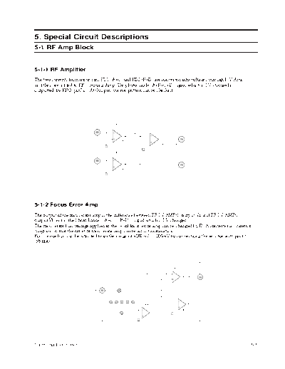
5. Special Circuit Descriptions
5-1 RF Amp Block


5-1-1 RF Amplifier
The two currents from input pins PD1 (A+C) and PD2 (B+D) are converted into voltages through I/V Amp,
and they are added to RF summing Amp. The photo diode (A+B+C+D) signal which is I-V changed is
outputted by RFO (pin74). At this pin, the eye pattern can be checked.


                                                      58K


                          PD1   65                    -             VA 10K
                                                                                           -
                                                      +                                                               74     RFO
                                                            IV AMP
                                                                                           +
                                     VC                                                        RF SUMMINGAMP
                                                                                     VC
                                                      58K


                          PD2   66                    -
                                                                    VB 10K
                                                                                                                      73     RF-
                                                      +
                                                            IV AMP
                                     VC


5-1-2 Focus Error Amp
The output of the focus error amp is the difference between RF I-V AMP(1) output Va and RF I-V AMP(2)
output Vb,just is the Photo Diode ((A+C) - (B+D)) signal which is I-V changed.
The focus error bias voltage applied to the (+) of focus error amp can be changed by D/A converter as shown in
diagram, so that the offset of focus error amp can be adjust automatical.
Focus error bias can be adjusted from the range of +100mV ~ -100mV by connectiong the resistor with pin 63
(FEBIAS).


                                                                                                           164K

                                                                                     32K
                                                                    VB>                                    -
                                                                                     32K                                             59   FE1
                                                                    VA>                                    +
                                          sev-stopb
                                                                                                    160K
                                                               SW1
                           FEBIAS    63
                                              sev-stop
                                          <5 Bit Counter>                                           4K

                                                                                     3K                           -
                                                                                                                             fcmpo
                                                  X1      X2   X4     X8   X16
                                                                                                                  +
                                                                                 -

                                                                                 +         FEBIAS          VC     fe-stopb


Samsung Electronics                                                                                                                             5-1
Special Circuit Descriptions


5-1-3 Tracking Error Amp
The current signals from the side spot photo diode (E and F) are input to the E and F pin and converted into
voltage signals by E I-V and F I-V AMP. The output of tracking error amp is due to the difference between
E I-V AMP voltage output.
The E-F balance can be adjusted by modifying the gain of E I-V AMP, and the tracking gain(Pin TE1) can be
adjusted automatically by micom program.


                                                                                              TE1               LPFT

                                                                                              54                55


                     F   67             IV AMP                        -                                                                         BALL
                                                                                                                 -                  WIN COMP
                         68             IV AMP                        +                                                                         BALH
                     E
                              TGFI                     GAIN-UP/DOWN                                                            To ISTAT,TRCNT
                                                                                                                                                 TGL
                     EI 79                                                                                                          WIN COMP
                                                                                                  7.5K

                                                                                                         3.3K


                                                                                                                 1.5K
                                                                                            16K
                                                                                      13K


                                                                                                                                                 TGH
                                                         56K

                                                                27K


                                                                          13K
                                         220K

                                                110K
                                 75K


                                       BAL< 4 0 >
                                       GAIN< 3 : 0 >
                                 from Digital


5-1-4 Focus OK Circuit

Extracting the DC part of RFI and RFO and comparing with the basic DC level, if RF Level is more than basic
level, the FOK is output. The focus OK circuit generates a timing window of focus on to monitor the focus
search status of focus serve.


                                                                                40K

                                                               40K
                                                74                              -                        57K
                                                                                                                                      -
                                                75                              +                                                                      40   FOK
                                                           40K                                                                        +
                                                                                                                        90K


                                                                                                                        VC+0.625V


   5-2                                                                                                                                                            Samsung Electronics
                                                                                                                          Special Circuit Descriptions


5-1-5 Mirror Circuit
After RFI signal is amplified by mirror amp, mirror signal is held in peak and bottom circuit. The following of
100KHZ traverse is possible in peak hold circuit and the loss of track count due to defect is counted in bottom
hold circuit. Mirror output beyond 2KHz is. 


◦ Jabse Service Manual Search 2024 ◦ Jabse PravopisonTap.bg ◦ Other service manual resources online : FixyaeServiceinfo