Service Manuals, User Guides, Schematic Diagrams or docs for : Samsung GSM Samsung SGH-A200 service manual

<< Back | Home

Most service manuals and schematics are PDF files, so You will need Adobre Acrobat Reader to view : Acrobat Download Some of the files are DjVu format. Readers and resources available here : DjVu Resources
For the compressed files, most common are zip and rar. Please, extract files with Your favorite compression software ( WinZip, WinRAR ... ) before viewing. If a document has multiple parts, You should download all, before extracting.
Good luck. Repair on Your own risk. Make sure You know what You are doing.


Image preview - the first page of the document
Samsung SGH-A200 service manual


>> Download Samsung SGH-A200 service manual documenatation <<

Text preview - extract from the document
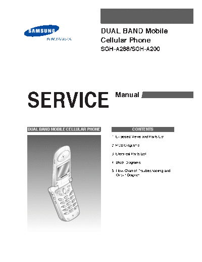
                                                             DUAL BAND Mobile
        ELECTRONICS
                                                             Cellular Phone
                                                             SGH-A288/SGH-A200


SERVICE                                                           Manual


DUAL BAND MOBILE CELLULAR PHONE                                               CONTENTS
                                                                1. Exploded Views and Parts List

                                                                2. PCB Diagrams

                                                                3. Electrical Parts List

                                                                4. Block Diagrams

                                                                5. Flow Chart of Troubleshooting and
                                                                   Circuit Diagram


                                              F
                     C                      DE

                             C
                           AB                    MN
                                                   O


                                  L
                                JK                      YZ
                                                      WX
                 I
               GH                       V
                                      TU

                       S
                    PQR
5. Flow chart of trouble shooting and Circuit Diagram

5-1 Power ON


               'POWER ON'does not work


                                Yes

               Check the Battery Voltage       No
                                                                Charge the Battery
                   is more than 3.2V


                                Yes


                     The node                  No     Check U116 and the path from +VBATT
          between D110 and BAT101 = 3V ?
                                                                   to BAT101


                                Yes

                                               No
                U117 pin 1,4,10 > 3.2V                   Check the circuit related to U117


                                Yes

                                               No
                  U463 pin 1, 3 = "H"?                   Check the circuit related to U463


                                Yes

                                               No
                 U463 pin5, 7 = 2.9V ?                    Check U463 and related circuit


                                Yes

                                               No
                                                        Check the clock generation circuit
          Check for the clock signal at R301
                                                           (related to U303 and U301)


                                Yes

               Check the initial operation


                          END


5-1                                                 Flow chart of trouble shooting and Circuit Diagram
                                                                                                                                                                     U116
                                                                                                                                                               1           5
                                                     +VBATT                                                                                                        VINVOUT                                                                                               RTC_3V3
                                                                                                                                                               2 GND

                                                                                                                                                               3   BYPASS 4                       C208
                                                                          C699                                                                                    ON/OFF                                                 C211
                                                                                                                                                                                                                                                                         RTC_VCC
                                                                                                                                       C190


                                                                                                                                                                                                                                                       1
                                                                                                                                                                                                                                                                  C713
                                                                                                                                                                                                                                           BAT101
                                                                                     L102           D108
                                                                                                                                           3.3V


                                                                                                                                                                                                                                                       2
                                                                        U117                               C209    C202
                                                                                   R164
                                                               1 FB       OUT 10
                                                               2 LBI       LX 9
                                                               3 _LBO     GND 8                                                                                               VCC                                 AVCC
                                                               4 CLSEL BATT 7                                                                           U463
                                                                                                                                            5                       4


Flow chart of trouble shooting and Circuit Diagram
                                                               5 REF    _SHDN 6                                                                   PS1     GND
                                                                                                                                            6                       3
                                                                                                                                                  PS2/3    VO1
                                                                                                   C746                                     7                       2
                                                              C203                                                                                NO      VO2
                                                                                                                                            8                       1
                                                                                                                                                  VIN     VO3

                                                                                                                                                                                                                    C328         C555

                                                                                                                                                                            C535           C700            C708


                                                                                                                                                                                      One Point Contact
                                                                                                                                                                                                                   One Point Contact
                                                                                                                                D107
                                                                                                                                       1
                                                                                                                                                                                                                                                                         BB_PWR
                                                                                                                                       3
                                                                                                                            2                                                                                                                                            ON_OFF
                                                                                                                                       4

                                                                                                                                       5

                                                                                                                     C701                                                                                                                                                RTC_3V3
                                                                                                            R567


                                                                                                                                                                                                                           3                    R157
                                                                                            DCIN                                                                                                                                       1
                                                                                                                                                                                                                                                                         DCVOLT
                                                                                                                                                                    R166       C186      R167       R168
                                                                                                                                                                                                                           2
                                                                                                                                                                                                                                   U111

                                                                                                                                                                                                                                                           R161


5-2
5-2 Initial


              Initial Failure


                                       No   Check and repair the important
            U103 pin 4 = "H" ?
                                              signals of U108 as follows


                       Yes
                                                     The node                No
                                               between R162 and C183                  Check U112
                                                     = "H" (RST)

                                                             Yes


                                                                             No
                                                 R114 = "H" (BOOT)                   Resolder R114


                                                             Yes
      Check all the other connection
                by Test S/W
                                                                             No
                                                 R673 = "H" (MSIZE)                  Resolder R673


                                                             Yes
      Check the circuit around LCD

                                                                             No
                                                R165 = "L" (EXTPROC)                 Resolder R165


            Check the circuit
         around U107(EEPROM)
           and data stored in it
                                                    Replace PBA


                   END


5-3                                                       Flow chart of trouble shooting and Circuit Diagram
                                                                                                  U108
                                                                                                                                         U109          VCC
                                                              U645
                                                                                                                                                          Q108
                                                                           R162
                                                                                         SYSRST
                                                                                                                                  6   F_BE0                             F_WP
                                                                                  C183                                                        F_VCCW
                                                                                                                                                                 R156
                                                                                                                 VCC


Flow chart of trouble shooting and Circuit Diagram
                                                                                                                                  4   F_BE1            R163


                                                                      VCC                                          R673


                                                                                                         GPIO4            MSIZE
                                                                    R114


                                                     SIMPWDN_BOOT                        GPIO3

                                                                                                          DTR1            F_WP


5-4
5-3 Charging Part


              Abnormal charging part


                              Yes


                                                No
        Check the CN502 pin 17,18      5.2V ?                     Replace TA


                              Yes


                                                No
          Check the U639 pin 3      5.2 V ?               Resolder C111, L632, C710


                              Yes


                                                No
                 U639 pin 4 = "L" ?                             Resolder R328


                              Yes


                                                No
                                                         Resolder components around
          Check the U639 pin 5      4.2V ?
                                                                    U639


                              Yes


                        END


5-5                                              Flow chart of trouble shooting and Circuit Diagram
                                                                                                                                                   +VBATT


                                                                                                                 Q303          R320
                                                                                                                        3
                                                                                             U639            1
                                                                                                                                                   BAT_VOLT
                                                                                   1                     6              2
                                                                                       ISENSE    DRIVE


Flow chart of trouble shooting and Circuit Diagram
                                                                                   2                     5                     R671         C704
                                                                     L632              GND      VSENSE

                                                     DCVOLT                        3   VCC       PROG
                                                                                                         4


                                                              C111          C710                                                                   ICHRG


                                                                                                                        R328


                                                                                                                                      L:ON,H:OFF
                                                                                                                                                   CHG_ON


5-6
5-4 Sim Part


                   Phone can't access SIM card

                                     Yes

                                                       No
                          R699 = 2.9 V ?                        Check the circuit related to U463


                                     Yes

                                                       No
                                                                  Check the circuit related to
                        U463 pin1 = 3 V ?
                                                                      R421, R428, U649


                                     Yes

                                                       No
                        U101 pin6 = 3 V ?                                Resolder R103


                                     Yes

                                                       No
                        U101 pin 5 = "H" ?                              Replace the PBA


                                     Yes

                                                       No
                      U101 pin 2, 3 = 3 V ?
                                                                         Replace U101


                                     Yes

                                                       No             Resoldering CN102
                      CN102 pin 1, 5 = 3 V ?                      and check open connection
                                                                     from U101 to CN102


                                     Yes


                        After Power ON,                No
               Check SIMCLK Signal on CN102 pin 3                        Replace PBA
                        in a few second


                                     Yes


                                                       No
                      After SIM card insert,
                   CN102 pin 2 = "H(SIMRST) ?                           Replace the PBA


                                     Yes


                  Check the circuit around U107
               (Serial EEPROM) and data stored in it


                               END


5-7                                                         Flow chart of trouble shooting and Circuit Diagram
                                                                                  VCC                                       SIM_VCC                                    SIMDATA


                                                                                                                                                                                                              C751
                                                                                                                                                                                          R698

                                                                                    R699                                                        U101


Flow chart of trouble shooting and Circuit Diagram
                                                                                                            U649
                                                                                                  6                  1            R103                  3
                                                                                                                                          4   VIN,R1
                                                                                                      VIN     VOUT                                     V.C1-2
                                                                                                  5 C1+      2                            5 ON/OFF      2
                                                                                                         GND                                                                                        CN102
                                                                           C423                                                                  V.C1-1 1
                                                                                                  4          3                            6 R1,C1
                                                                                                                                                    R2                                            1 C1 C5 4
                                                                                                    C1- MODE             C745                                   C107
                                                                                           C424                                 C104                                      SIMRST
                                                                                                                                                                                                  2 C2 C6 5
                                                                                                                                                                                                  3 C3 C7 6
                                                                                                                                         FDG6323L                         SIMCLK
                                                                    R421
                                                         SIM_5V3V
                                                                                                                                                                                   C749    C750               C748
                                                     SIMPWDN_BOOT
                                                                    R428

                                                          SIMALIM


5-8
5-5 Microphone Part


            Microphone does not work


                            Yes


                     Check                 No
                                                    Resolder CN503 pin 10, 11 and
                 the connection
                                                           ZD109, ZD112
             from CN503 pin 10, 11


                            Yes


                                           No
        U113, U115 pin 2 (AVCC)    2.9V?           Check the circuit related to U463


                            Yes


                                           No
                Check the circuit                  Resolder the R174, R175, R176,
            from U108 to U113, U115                 R177, C187, C188 and C204


                            Yes


                                           No
               Check the Key PCB                        Replace the Key PCB


                            Yes


                      END


5-9                                         Flow chart of trouble shooting and Circuit Diagram
                                                                CN503

                                                                        10

                                                                                    ZD112


                                                                        11


                                                                                    ZD109


                                                                             AVCC


Flow chart of trouble shooting and Circuit Diagram
                                                                                         U115
                                                                                                                AVCC

                                                                                                6


                                                                AVCC                                                            U108
                                                     U463                            2
                                                                                                             R177

                                                                                                    R176               C188

                                                                                                5                             VXI1P


                                                            3
                                                                                     U113
                                                                                                      R175             C187
                                                                                                5                             VXI1N


                                                                                                             R174
                                                                                     2


                                                                                                6


5-10
5-6 Speaker Part


           Speaker does not work


                           Yes


                                       No
             J101 pin 2, 3 = short                          Resoler J101


                           Yes


                                       No
            J101 pin 2, 3, 6 = 1.5V?                     Replace the PBA


                           Yes


                                       No
           CN 105 pin 22, 23 = 1.5V?                     Resolder CN105


                           Yes


                    Check              No
              the depression of                        Modify the SPK pins
                 the SPK pins


                           Yes


                                       No
             Is Speaker working?                       Replace the Speaker


                           Yes


                     END


5-11                                        Flow chart of trouble shooting and Circuit Diagram
5-7 Key Data Input


                    Check Initial operation


                                    Yes


                              Are                    No
                  the pin 19,20,21,22 and 23                     Replace the PBA
                        of CN503 low?


                                    Yes


                              When
                                                     No
                   one of the keys is pushed,             Resolder pin 19,20,21,22 and 23
                one of pin 19,20,21,22 and 23 of                    of CN503
                         CN503 is high ?


                                    Yes


                                                     No
                       Key PCB is OK ?                         Replace the Key PCB


                                    Yes


                              END


Flow chart of trouble shooting and Circuit Diagram                                          5-12
5-8 Alert Tone


                 Abnormal Alert tone


                                              No
          Is there alert wave form on the
                                                            ALERT by Test S/W
            R110 during alert tone test?


                              Yes


                                              No
          Is there alert wave form on the
                                                      Check the circuit related to Q102
         Q102 pin 3 during alert tone test?


                              Yes


                                              No
                 U116 pin 5   3.3V?                   Check the circuit related to U116


                              Yes


                                              No
                    Buzzer is ok?                            Change the Buzzer


                              Yes


                        END


5-13                                           Flow chart of trouble shooting and Circuit Diagram
                                                                                  RTC 3V3(From U116 pin5)


                                                                                                                   BUZ+

                                                                                                            C102
                                                                                     D104


Flow chart of trouble shooting and Circuit Diagram
                                                                             Q102                                  BUZ-
                                                               R110                    3
                                                                              1
                                                     From IC
                                                                                       2
                                                                      R109


5-14
5-9 Ring Indicator


           Ring Indicator LED does not
                       work


                                         No
                Q101 pin 2 = "H"?                         GPO2 by Test S/W


                            Yes


                                         No
                Q101 pin 3 = "L"?                          Replace Q101


                            Yes


                                         No
               CN503 pin 3 = "L"?                       Resolder CN503, LED


                            Yes


                                         No
                 Key PCB is OK?                         Replace the Key PCB


                            Yes


                      END


5-15                                      Flow chart of trouble shooting and Circuit Diagram
                                     KPCB A'SSY
                                     CN503


                                                  3  Q101


                                                                      R706
                                                            (From U108)
                                                              RI_LIGHT


Flow chart of trouble shooting and Circuit Diagram                           5-16
5-10 Back Light


                           Backlight does not work


                                                                  No
                            Backlight "ON" mode
                                                                           Select backlight "ON" mode
                               in the menu?


                                          Yes


                                                                  No
                                  R141 = "H" ?                                   GPO1 by test S/W


                                            Yes
             LCD BACKLIGHT                                        KEY PCB LED


                                                  No
                                                                   Check the
       Check the CN105 pin 17 = "H" ?
                                                                  CN105 pin 17


                          Yes


                                                  No
             LCD backlight on ?                                  Replace EL sheet


                          Yes
                                                                              No
                                            Resolder R141, R149                                Q107 pin 1 = "H" ?
                    END

                                                                                                          Yes


                                                                              No
                                                 Resolder Q107                                 Q107 pin 3 = "L" ?


                                                                                                          Yes


                                                                             No
                                              Resolder CN503
                                                                                               Key PCB LED on ?
                                            or Replace Key PCB


                                                                                                          Yes


                                                                                                        END


5-17                                                                   Flow chart of trouble shooting and Circuit Diagram
5-11 GSM Receiver

                                 Rx On
                  RF input : CH center freq. + 67.7 kHz
                              Amp. : -50 dBm


                                  U304                    No    Check RF connector
                                  Pin 2
                                                                    -> resolder
                                 -65 dBm


                                       Yes

                                                                                                                    Check
                                  U304                         No                       Resolder &       No        VC1 : L
                                  Pin 9                                                 U304 Pin 9
                                                                                                                   VC2 : L
                                 -65 dBm                                                 -65 dBm
                                                                                                                   VC3 : H


                                       Yes                                                    Yes


                                  U603                    No          Resolder
                                  Pin 7                                U603
                                 -70 dBm


                                       Yes

                                  F303                    No                Resolder
                                  Pin 2                              L613, L635, L639, C695
                                 -60 dBm


                                       Yes

                                  U305                    No            Resolder
                                Pin 53, 54                             F303, C333
                                 -60 dBm                               L323, L324


                                       Yes
                                                                                            Check
                                  U305                                                 C301(CH+225MHz)
                                Pin 49, 50                     No                                             No       Resolder
                                                                                            -20 dBm
                                (225 MHz)                                                                               U302
                                                                                        C315(1080MHz)
                                 -50 dBm                                                    -20 dBm

                                       Yes                                                       Yes


                                  U305                                Resolder
                                Pin 43, 44                No
                                                                U601,C309,C310,C312
                                (45 MHz)                        C313,C314,C400,R700
                                 -55 dBm

                                       Yes

                                  U305                    No            Resolder
                            Pin 24, 25, 26, 27                      OneC(U108), U305
                                  40 mV


                                       Yes

                             Check U305                   No           Resolder
                             Pin 32, 33  2.5 V                  U305 (Pin35, Pin 32, 33)
                               Pin 35  0.5 V


                                       Yes
                                 Resolder
                                  U108


Flow chart of trouble shooting and Circuit Diagram                                                                                5-18
5-12 GSM Transmit


              Tx On (level : 5)


                     U304             Yes           Resolder
                     Pin 2
                                                     J301
                    30 dBm


                           No

                                                                  Check
                     U304                   Yes                  VC1 : H              Yes      Change or Resolder
                     Pin 7                                       VC2 : L                             U304
                    30 dBm                                       VC3 : L


                           No                                            No
                                                                                                Check
                                      Yes                                             Ant. S/W, Control Circuit
                     U312                          Resolder
                     Pin 4
                                                  U318, C353
                    30 dBm


                           No

                                                                         Check
                     U312             Yes                            U312 : +VBATT      Yes           Resolder or
                     Pin 1                                            Pin 2 (APC)                    Change U312
                     0 dBm                                                OK?
                                                                                 No           Check +VBATT
                           No                                                                 or APC Control


                     U200             Yes             Resolder or Change
                     Pin 6                          C698, R335, R364, R366
                     7 dBm


                           No

                      U200            No
                    Pin 7  0.5 V
                                                      Resolder
                    Pin 5  2.8 V                  U108, U457, U200
                  Pin 3 = 0.5~2.5 V


                             Yes

                       U305           No              Resolder
                    pin 30, 47
                                                       U302
                     -10 dBm


                             Yes

                      U305             No            Resolder
                Pin 17, 18, 19, 20                  OneC(U108)
                      40 mV


                             Yes


                 Check U305           No           Resolder
                  Pin 38  2.5 V               U305 (Pin35, Pin38)
                  Pin 35  0.5 V


                             Yes
                    Resolder
                     U108


5-19                                                             Flow chart of trouble shooting and Circuit Diagram
5-13 DCS Receiver

                             Rx On
              RF input : CH center freq. + 67.7 kHz
                          Amp. : -50 dBm


                              U304                    No        Check RF connector
                              Pin 2
                                                                    -> resolder
                            -65 dBm


                                   Yes

                                                                                                                 Check
                              U304                         No                          Resolder &      No        VC1 : L
                             Pin 16                                                    U304 Pin 16
                                                                                                                 VC2 : L
                             -65 dBm                                                     -65 dBm
                                                                                                                 VC3 : H


                                   Yes                                                        Yes


                              U603                    No          Resolder
                              Pin 5                                U603
                             -70 dBm


                                   Yes

                              F302                                 Resolder
                              Pin 2                         C627, C724, C725, L636
                             -60 dBm


                                   Yes

                              U305                    No            Resolder
                            Pin 2, 3                               F302, C335
                             -60 dBm                               L638, L637


                                   Yes
                                                                                          Check
                              U305                                                   C301(CH-225MHz)
                            Pin 49, 50                     No                                               No     Resolder
                                                                                          -20 dBm
                            (225 MHz)                                                                               U302
                                                                                      C315(1080MHz)
                             -50 dBm                                                      -20 dBm

                                   Yes                                                         Yes


                              U305                                Resolder
                            Pin 43, 44                No
                                                            U601,C309,C310,C312
                            (45 MHz)                        C313,C314,C400,R700
                             -55 dBm

                                   Yes

                              U305                    No            Resolder
                        Pin 24, 25, 26, 27                      OneC(U108), U305
                              40 mV


                                   Yes

                         Check U305                   No                Resolder
                         Pin 32,33  2.5 V                       U305 (Pin 35, Pin 32, 33)
                          Pin 35  2.5 V


                                   Yes
                             Resolder
                              U108


Flow chart of trouble shooting and Circuit Diagram                                                                            5-20
5-14 DCS Transmit

             Tx On (level : 0)


                    U304            Yes          Resolder
                   Pin 2
                                                  J301
                   25 dBm


                           No

                                                                 Check
                    U304                  Yes                   VC1 : L            Yes      Change or Resolder
                  Pin 13                                        VC2 : H                           U304
                   25 dBm                                       VC3 : L


                           No                                        No
                                                                                             Check
                                                                                   Ant. S/W, Control Circuit


                    U312            Yes          Resolder
                   Pin 5                        U318, C364
                   25 dBm


                           No

                                                                      Check
                    U312                   Yes                    U312 : +VBATT       Yes         Resolder or Change
                    Pin 8                                          Pin 2 (APC)                           U312
                    0 dBm                                              OK?


                           No                                                 No            Check +VBATT
                                                                                            or APC Control


                    U200            Yes            Resolder or Change
                   Pin 10                        C697, C346, R365, R363
                   10 dBm


                           No

                    U200
                  Pin 7  2.5 V      No          Resolder
                  Pin 5  2.8 V
                Pin 3 = 0.5~2.5 V           U108, U457, U200


                            Yes

                     U305           No
                   pin 30, 47                   Resolder U302
                    -10 dBm


                            Yes

                    U305            No             Resolder
              Pin 17, 18, 19, 20                  OneC(U108)
                    40 mV


                            Yes


               Check U305           No           Resolder
                Pin 38, Pin 35              U305 (Pin35, Pin38)
                    2.5 V


                            Yes
                   Resolder
                    U108


5-21                                                              Flow chart of trouble shooting and Circuit Diagram
                                                                            R312
                                                                             10
                                                     XVCC

                                                                                                    C319
                                                                                                    10NF

                                                                                                                           C305            L303
                                                                                                                           5.6NF           27nH

                                                                                        U303
                                                              R313
                                                               1K                  1            4
                                                      AFC                              VT VCC
                                                                                                                  R308
                                                                                   2            3                  1K
                                                                                       GNDOUT
                                                                     C320
                                                                     10NF                                  C306
                                                                                                           10NF
                                                                                                                                                      U301
                                                                                                                                           4                              3
                                                                                                                                           5
                                                                                                                                                                              2                                                                 C302
                                                                                                           R305                                                                                                                          R301
                                                                                                            1K                                                                                                                           1.5K   1NF
                                                                                                                                           6                                  1
                                                                                                                                                                                                                                                                       CLK13M
                                                                                                                                               UMZ1N-TR
                                                                                                                                   R304
                                                                                                                                                                                                                        R303
                                                                                                                                                                                                                        1K


                                                      3VRF


Flow chart of trouble shooting and Circuit Diagram
                                                                                                                                                                                                                            R302
                                                                                                                           R311
                                                                                                                            0                                                                                                 0

                                                                                       C304
                                                                                       100NF                                                                                                                                    C303
                                                                                                                                                                                                                                100NF
                                                                                                                   C316            C308
                                                                                                                   100NF           100NF


                                                                                                                                                                                                                                                       L301    C301
                                                                                                                                                                                                                                                               560PF
                                                                                                                                                                                                                                                       2.2nH
                                                                                                                                                                                                                                                                          RFLO


                                                                                                                                               14 13 12 11 10                                           9        8

                                                                                                                   C307


                                                                                                                                                  NC
                                                                                                                                                                                                                     NC
                                                                                                                    1NF


                                                                                                                                                                                                          GNDR


                                                                                                                                                                                      VDDR
                                                                                                                                   15                                                                                                7


                                                                                                                                                               PWDNB
                                                                                                                                                                                               RFOUT
                                                                                                                                        XIN                                                                             GNDR


                                                                                                                                                                          AUXOUT
                                                                                                                                   16                                                                                                6
                                                                                                                                        GNDD                                                                              RFLA
                                                                                                                                   17                                                                                                5
                                                                                                                                        VDDD                                                                              RFLB
                                                                                                                                   18                                                                                                4
                                                                                                                                        GNDD                                       U302                                 GNDR
                                                                                                                                   19                                  SI4133-MLP28                                                  3
                                                                                                                                        IFLA                                                                              RFLC
                                                                                                                                   20                                                                                                2
                                                                                                                                        IFLB                                                                              RFLD
                                                                                                                                   21                                                                                                1
                                                                                                                                        NC                                                                                      NC


                                                                                                                                                                       VDDI

                                                                                                                                                       IFOUT
                                                                                                                                               GNDI
                                                                                                                                                                                             SCLK
                                                                                                                                                                                                       SDAT


                                                                                                                                                                                   SENB
                                                                                                                                                                                                                 GNDR
                                                                                                                                                                                                                          GND


                                                                                                                                           22 23 24 25 26 27                                                  28 29
                                                                                                                                                                                                                                                       L304    C315
                                                                                                                                                                                                                                                       10nH    560PF
                                                                                                                                                                                                                                                                          IFLO


                                                                                                    R310
                                                                                                    1.5K
                                                     SYNEN1

                                                       SCLK


                                                      SDATA


5-22
5-23
                                                         RFLO
                                                       AGC_EN
                                                         SCLK
                                                        SDATA                                                                                                                                                                                                                                                                                                                                                 3VRF

                                                                                                                                                                      R370        C337       C344
                                                                                                                                                                       22                                                       C321
                                                                                                                                                                                  27PF       1NF                                                  L305                 L306


◦ Jabse Service Manual Search 2024 ◦ Jabse PravopisonTap.bg ◦ Other service manual resources online : FixyaeServiceinfo