Service Manuals, User Guides, Schematic Diagrams or docs for : Samsung LCD TV LE32A559P4FXXC SAMSUNG__TFT_LCD_TV_LE32A559P4FXXC.part4
<< Back | HomeMost service manuals and schematics are PDF files, so You will need Adobre Acrobat Reader to view : Acrobat Download Some of the files are DjVu format. Readers and resources available here : DjVu Resources
For the compressed files, most common are zip and rar. Please, extract files with Your favorite compression software ( WinZip, WinRAR ... ) before viewing. If a document has multiple parts, You should download all, before extracting.
Good luck. Repair on Your own risk. Make sure You know what You are doing.
Image preview - the first page of the document
>> Download SAMSUNG__TFT_LCD_TV_LE32A559P4FXXC.part4 documenatation <<
Text preview - extract from the document
7. Schematic Diagram
7. Schematic Diagram
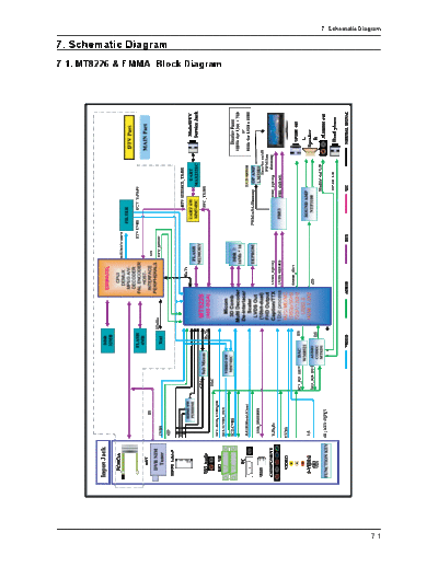
7-1. MT8226 & EMMA Block Diagram
7-1
7. Schematic Diagram
The Block Processing Video Signal
1. Component, PC and CVBS signal like AV are inputted to Scaler-IC (MT8226(IC5105)) directly.
2. HDMI signal is inputted to switch-IC, TMDS351 to select just 1-HDMI input in 3-HDMI input.
(But HDMI3 (Side) inputted to Scaler-IC directly), And then Selcted HDMI signal is inputted to Scaler-IC.
3. Scaler-IC converts video signal to 12bit of LVDS Signal, standard format to run a LCD panel.
4. FBE3-IC receives this LVDS signals and processing it to enhamce picture quality.
And then final 12bit of LVDS Signal is outputted.
The Block Processing Sound Signal
1. Sound signals of RF(SIF), HDMI, Component, DVI, PC and AV input are inputted to
Sound-IC (MT8291 (IC2102)).
DTV_AUDIO signal is also inputted for MP3 connected to wiselink.
MT8291(IC2102) processes these signal and outputs 12C signal to digital AMP-IC (NTP3100 (IC2104)).
And signals for headphone and Monitor-out are outputted.
2. NTP-3100 IC outputs an analog sound signal to run Speakers.
7-2
7. Schematic Diagram
7-3. Schematic Diagrams
7-3-1. MAIN POWER BLOCK
7-3
7. Schematic Diagram
7-3-2. SOUND
7-3-3. Jack_In_Out-1 & Function
7-4
7. Schematic Diagram
7-3-4. Jack_In_Out-2 & HDMI_Switch
7-3-5. Jack_In_Out-3 & Tuner
7-5
7. Schematic Diagram
7-3-6. Scaler-1 & Flash memory & Sub-Micom
7-3-7. Scaler-2 & Main-DDR
7-6
7. Schematic Diagram
7-3-8. Scaler-Power & Service
7-3-9. FBE3 & LVDS Out
7-7
7. Schematic Diagram
7-3-10. Emma2 & DTV-DDR
7-3-11. Emma2SL & PCMCIA & Flash memory
7-8
◦ Jabse Service Manual Search 2026 ◦ Jabse Pravopis ◦ onTap.bg ◦ Other service manual resources online : Fixya ◦ eServiceinfo