Service Manuals, User Guides, Schematic Diagrams or docs for : Samsung Plasma PPM-42S3QX chassis D61B PPM-42S3Q ch.D61B_training Trouble Shooting

<< Back | Home

Most service manuals and schematics are PDF files, so You will need Adobre Acrobat Reader to view : Acrobat Download Some of the files are DjVu format. Readers and resources available here : DjVu Resources
For the compressed files, most common are zip and rar. Please, extract files with Your favorite compression software ( WinZip, WinRAR ... ) before viewing. If a document has multiple parts, You should download all, before extracting.
Good luck. Repair on Your own risk. Make sure You know what You are doing.


Image preview - the first page of the document
Trouble Shooting


>> Download Trouble Shooting documenatation <<

Text preview - extract from the document
                                                                                                       Troubleshooting


7 Troubleshooting
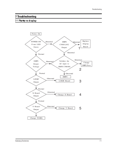
7-1 Partly no display


                       Power On


                       POWER ON             Abnor mal         SMPS                        Replace
                                                                             Abnor mal
                       F ront LED                          CN8 0 1 ,8 0 2                 Display
                         Gre en                              Output                        Board
                                                                                    1
                                                                      Abnormal
                               Normal


                                                                               Abnormal
                         SMPS               Abnormal      Validate the
                                                                                           Change
                         Output                           AC input to
                                                                                          SMPS Fus e
                        Volta ge                         SM PS CN8 0 0 S

                                                                                     2
                                   Normal                          Abnor mal
                                                               SMPS
                         LOGIC               Abnor mal

                         Output
                                                          LOGIC Board
                                                                                     3

                               Normal
                                              Abnormal
                        X - Board
                         Output
                                                         Change X - Board            4
                                Normal


                        Y - Board            Abnormal
                         Output
                                                          Change Y - Board           5

                      Change PANEL


Samsung Electronics                                                                                               7-1
Troubleshooting


                  Partly no dis play.


      Symptom


                  1 ) 2 Half of s cre en doe s n't appea r    2 ) 3 Vertically,1 /7 of s cree n does n't appe ar
      Ca us e     Some buffer boa rds doe s n't work correctly.
                           POWER ON


                           Lowe r Part
                                                                     Re pla ce Lowe r Buffe r board
                            No Scre en
                                                       1


                                 1 /2
                                                                     Replace Lowe r Sc an board
                            No Scre en
      T rouble                                        2
      Shooting


                           Vertical(1 /7 )
                                                                    Re place Addre s s buffe r board
                            No Scre en
                                                          3


                           Vertical(3 /4 )
                                                                            Replace PANEL
                            No Scre en
                                                       4


                                                   No 1 , Replace Lower Buffer Board


                                                   No 3 , Replace Addres s buffer boa rd


7-2                                                                                               Samsung Electronics
                                                                                                             Troubleshooting


                      No Dis play ( Ope rating Voltage s e xis t ,but an Image doesn't exist on Screen.


    Symptom


    Ca use            F u se or FET is de stroyed.


                                                     [ Y- MAIN ]
                                                C he ck s eve ral point s


                         F50 0 3 for Vs
                                                                              OPEN
                         F50 0 2 for Vcc                 FUS E                               Re place the board
                         F50 0 1 for Vdd

    T rouble                                                      OK
    Shooting             Q5 00 9 ~ Q50 1 0
                                                                             SHORT
                         Q5 01 2 ~ Q50 1 5                FET                                Repl ace the b oard
                         Q5 01 7 ~ Q50 2 4

                                                                  OK


                                                       Y- MAIN
                                                     Normal State


                       < Y- MAIN B OARD>


    F USE


                        FUSE


    F ET


                            F 5 00 1 ~ 3                                    F 5 00 9 ~ 2 4


Samsung Electronics                                                                                                     7-3
Troubleshooting


                  No Display ( Op e rating Voltages exis t, but an Image doe sn't exist on Screen. )


      Symptom


      C au se     F use or FET is destroyed.


                                               [ X- MAIN ]
                                          Che ck seve ra l po int s

                                                                      OPEN
                                                                                Re plac e the
                                                   FUS E
                                                                                   bo ard
                                                            OK
      T rouble      F40 0 3 for Vs
                                                                      SHORT
                    F40 0 1 for Vcc                 FET                         Replace the
      Shooting
                    F40 0 2 for Vdd                                                 boa rd

                    Q4 00 9 ~ Q40 1 6                       OK

                                                 X- MAIN
                                                                              Che ck Logic- main
                                               Normal St ate


      F USE


                   F USE


      F ET


                                                 Q4 0 0 9 ~ 1 6


7-4                                                                                          Samsung Electronics
                                                                                                      Troubleshooting


                      No Display (Op er ating Volta ge s e xis t , but an Image doesn't exist on Screen.)


    Symptom


    Caus e            Ve rt ica l sync on LOGIC- MAIN isn't normal.


                                    [ Logic Main ]
                              LED(LD200 0) blinks ?
                                   (action of Vsync)
                                                              NG
                                                                          Re place the board
    Trouble
    Shooting                                  OK

                                      Logic Main
                                                                             Replace PDP
                                     Normal S t ate


                         Blink ?


Samsung Electronics                                                                                              7-5
Troubleshooting


                  Abnormal Display Abnormal Image is on Scre en.
                  (exce p t abnormality in Su s tain or Addres s )

      Symptom


      C au se     F u s e or FET is de stroyed.


                                          [ Y- MAIN ]
                                      Check s evera l points


                  F50 0 3 for Vs                               OPEN
                  F50 0 2 for Vcc             FUSE                        Re pl a ce Y board
                  F50 0 1 for Vdd
                                                     OK

                  Q5 00 9 ~ Q50 1 0
                  Q5 01 2 ~ Q50 1 5            FET             S HORT     Repl ace Y board

                  Q5 01 7 ~ Q50 2 4
                                                     OK

                                             Y- MAIN
                                                                        Check X- main
                                          Normal State

      Trouble
      Shooting


                    < Y- MAIN         BOARD>


7-6                                                                                            Samsung Electronics
                                                                                                Troubleshooting


                      Abnormal Dis play Abnormal Image is on Scree n.
                      (e xcept abnormality in Sus tain or Addres s )

    Symptom


    Cau s e           F u se or FET is de s troye d.


                                               [ X- MAI N ]
                                           Chec k s e veral points


                      F40 0 3 for Vs
                                                                     NG
                      F40 0 1 for Vcc              FUS E                  Re place the b oard
                      F40 0 2 for Vdd

                                                          OK

                                                                     NG
                       Q4 00 9 ~ Q40 1 6            FET                   Replace the board


                                                           OK

                                                  X- MAIN                  Check Logic- main
                                               Normal State
    T rouble
    Shooting


                         < X- MAIN B OARD>


Samsung Electronics                                                                                        7-7
Troubleshooting


                  Dis play Abnormal Image is on Scre en .
                  (e xce p t abnormality in Sus tain or Addres s )


      Symptom


      Ca use      Action of Vs ync on LOGIC- MAIN is n't normal.


                          [ Logic Main ]
                       LED (LD2 000 ) blinks
                         (action of Vsync)


                             regula r                 NO
                                                                      Logic Main
                            abnorma l
                                                                     Norma l State
                              pattern


                                        YES

      T rouble
                           Replac e b oard                           Replac e PDP
      Shooting


7-8                                                                                  Samsung Electronics
                                                                                                  Troubleshooting


                      Some horizontal lines appear to be linked on Video


    Symptom


    Cau se            Su stain Short . De fect on F PC .


                                     [ Y- FPC ]
                                    Sust ain Open


                                    After Cha nging             NG
                                                                              Repl ace the pa ne l
                                 buffer, rec hec k the
                                                                           The re 's a de fec t on FPC
                                         s t at u s


                                                      OK

                                          Done
                               ( De f e ct is from buff e r )
    Trou ble
    Shooting


                          < FPC >


Samsung Electronics                                                                                          7-9
Troubleshooting


                   Some ve rtical lines appear to be linked on.


       Symptom


                      1 Line bla ck            1 Block is blac k        H alf of Sc ree n is blac k
       Cau se      Address Open

                     What is the status of open ?


                                                      NO                H alf bl oc k/
                              1 l i ne or
                                                                         HALF OF
                              1 block


       T rou ble
       Shooting                          YES                                       YES


                                                                   Re pl a c e Logi c Mai n
                             Rep l ace
                                                                     / A ddre s s Bu ffer
                               PDP                     NG          (E or F or G)/ FFC

                                                                                     OK

                                                                            DONE


                    < LOGIC - MAIN >


                     < E,F ,G ADDRES S BUFF ER B OARD >


7-10                                                                                          Samsung Electronics
Samsung Electronics
                                                                                                                                                                                              7-2 Logic Board
                                                                                                                                             7-2-1 Terms and Description of the Logic Board


                      !LVDS Connector : A connector which receives LVDS-encoded RGB, H, V, DATAEN and DCLK.
                      @Activity Indicator LED : Indicates that the Logic Board is receiving normal Sync and clock.
                                                 (Normal State: Blinks every second.)
                      #12C Connector : Connects with the Key Scan Board that checks and adjusts the 256K data.
                      $256K : An EEPROM that stores the Gamma Table, APC Table, Timing for driving waveforms, and other options.
                      %Y-Connector : A Connector which outputs the control signal for the Y Driving Board
                      ^X-Connector : A Connector which outputs the control signal for the X Driving Board
                      &CN401 (Left E-Address Buffer Connector) : Outputs the address data and control signal to the lower E-Buffer Board
                      *CN402 (Center F-Address Buffer Connector) : Outputs the address data and control signal to the lower F-Buffer Board
                      (CN403 (Right G-Address Buffer Connector) : Outputs the address data and control signal to the upper F-Buffer Board
                      )Power Connector : A power connector which receives the input power (5V) for the Logic Board
                      1Power Fuse : A fuse for the Power
                      2Optional Switch : It switches between Internal/External


7-11
                                                                                                                                                                                                                Troubleshooting
Troubleshooting


7-2-2 The Logic Board

The Logic Board consists of the Logic Main Board and the Buffer Board. The Logic Main Board processes
video signals to produce the Address Driver Output Signal and the Buffer Board delivers the Address
Driver Output Signal to the Address Driver IC (TCP Module).


                  Logic Board                                                  Function                            Remakr
                                                         Processes Video Signals (W/L, Error Diffusion, APC)
                  Logic Board                            Outputs the Address Driver Control Signal and the
                    (Main)                               Data Signal to the Buffer Board
                                                         Outputs the XY Driving Board Control Signal

 Buffer Board             E-Buffer Board - left side     Delivers the Data and Control Signal to the left TCP
 (Buffer Board,           F-Buffer Board - center        Delivers the Data and Control Signal to the center TCP
 on the back side)
                         G-Buffer Board - right side Delivers the Data and Control Signal to the right TCP


7-2-3 Waveform in a Normal State
When the PDP set is working properly and the Logic Board is normal, the Activity Indicator LED (as shown
in Fig. 1) blinks once per second.
Check the LED when the PDP has an error, and replace the Board if the LED status is abnormal.
If inspection of the board is required to clear a PDP unit error, refer to the Logic Board Inspection Guide for
the procedure (provided separately).


7-2-4 Diagnosis and Troubleshooting
A fault in the Logic Board can be caused by various reasons; follow the flow chart for troubleshooting.


          No Screen Image
                                                    Check the Input Power
                                           YES                                                     NO

                          Check the Activity Indicator LED
                                                                                              Check the Power Cable
                     NO                                  YES


       Check the Detailed Waveforms                                                              Check the Fuse
                                                  Replace the 256K and
       (Switch to the Internal Pattern.)          examine the PDP unit
                                                                                           Check the Power Unit Inductor

                                                 Check the Internal Pattern


                                             Check the Detailed Waveforms
                                             (Refer to the Inspection Guide)


7-12                                                                                                      Samsung Electronics
                                                                                                Troubleshooting


             Abnormal Screen Image


                                         Check the Activity Indicator LED


               Replace the 256K and examine the PDP unit          Check the Video Board

                                                                    YES

                          Check the Internal Pattern
                                                                Error of a particular TCP Block

                       Check the Detailed Waveforms               Check the Buffer Board
                       (Refer to the Inspection Guide)


7-2-5 Definitions of Terms
1. Logic Main Board
    Applies the PDP video signal by signaling the X, Y Driving Boards and the Logic E, F, G Buffers.
2. 5V, 3.3V
   5V : Voltage that is applied to the Logic Buffer by the Logic Main
   3.3V : Main voltage that is supplied to the Logic Main Board

7-2-6 Preparations Before the Inspection
1. Test Equipment / Measuring Instruments:
        Equipment must retain its precision and comply with regulations.
    Inspection Desk: 110V and 220V should be supplied, and there should be enough free space to hold the
                     instruments and test samples.
    Oscilloscope: A 500MHz Frequency Band with 2 or more channels is required.

7-2-7 Switch Descriptions of the Logic Main Board
1) Internal Pattern: Switch Off (Down Position) #2, #4 and Switch On #3 (Up) on SW2001
2) External Pattern: Switch On (Up) #2, #4 and Switch Off #3 (Down) on SW2001
* Switch to the internal pattern for board inspection
* 1 on SW2002 is not used.                                                 LOGIC BOARD
                                                                                               REMARK
                                                              M O DEL
                                                                             OPTION S/W
!Verify that the output voltages are 5V
                                                                                       ON
 and 3.3V when the SMPS is used.                               Inside
                                                                                                3 ON
@Set the oscilloscope to 4ms/div and 2V/div.                   42 SD                   OF F
 Connect Probe 1 as illustrated and set it to trigger.                       1 2 3 4
 Using Probe 2, analyze the waveforms at each point.
                                                                                       ON
                                                               Outside                           2, 4
                                                               42 SD                   OF F      ON
                                                                             1 2 3 4


Samsung Electronics                                                                                       7-13
Troubleshooting


7-2-7 Switch Descriptions of the Logic Main Board

1) Internal Pattern: Switch Off (Down Position) #2, #4 and Switch On #3 (Up) on SW2001
2) External Pattern: Switch On (Up) #2, #4 and Switch Off #3 (Down) on SW2001

* Switch to the internal pattern for board inspection
                                                                          LOGIC BOARD
* 1 on SW2002 is not used.                                 M O DEL
                                                                          OPTION S/W
                                                                                             REMARK


                                                                                    ON
                                                            Inside
!Verify that the output voltages are 5V                                                       3 ON
                                                            42 SD                   OF F
 and 3.3V when the SMPS is used.
                                                                          1 2 3 4
@Set the oscilloscope to 4ms/div and 2V/div.
 Connect Probe 1 as illustrated and set it to trigger.                              ON
                                                            Outside                             2, 4
 Using Probe 2, analyze the waveforms at each point.
                                                            42 SD                   OF F        ON
                                                                          1 2 3 4


                  GT 5           V _T OGG_M

         [Fig. 2] Connecting the Oscilloscope s Probe 1


#Turn the set ON to apply the 5V and 3.3V power to the Logic Main Board.
 Check whether the Vsync LED is blinking (located on top left side of the Logic Main Board).
 An LED that is blinking too fast or does not light up means the Logic Main Board is abnormal.
$Verify each waveform of the Logic Main Board and compare them to waveforms shown below.
 Each and every waveform should be verified.
%After finishing, turn off the power.
^When the inspection is finished, set SW2001 to the External Pattern.


7-14                                                                                     Samsung Electronics


◦ Jabse Service Manual Search 2026 ◦ Jabse PravopisonTap.bg ◦ Other service manual resources online : FixyaeServiceinfo