Service Manuals, User Guides, Schematic Diagrams or docs for : Samsung Plasma PS42 C 77 HD chassis F33B Wiring Diagram
<< Back | HomeMost service manuals and schematics are PDF files, so You will need Adobre Acrobat Reader to view : Acrobat Download Some of the files are DjVu format. Readers and resources available here : DjVu Resources
For the compressed files, most common are zip and rar. Please, extract files with Your favorite compression software ( WinZip, WinRAR ... ) before viewing. If a document has multiple parts, You should download all, before extracting.
Good luck. Repair on Your own risk. Make sure You know what You are doing.
Image preview - the first page of the document
>> Download Wiring Diagram documenatation <<
Text preview - extract from the document
Wiring Diagram
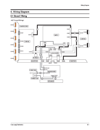
6. Wiring Diagram
6-1 Overall Wiring
<42" Overall Wiring>
CN5401
Y-MAIN SCAN
4 CN810
CN5402
CN4002
CN5407 CN809 5 CN4701
CN5707 SMPS
CN808
CN5403
X-DRIVE
CN5408 Y-DRIVE 6
CN800 CN801 CN807
CN5501 CN4001
CN5409 CN4004
11 7
CN2006 CN2001 CN2000
CN5412
CN5502 CN5701 CN2002 CN2003
?
LOGIC BOARD
2 CN2028 CN2004
AC-INLET 1
CN5503
E-BUFFER CN2509 CN2500 CN2600 CN2609 F-BUFFER
CN2510 CN2610
CN2202_HD
FUNCTION CN1101
CN1 MAIN BOARD
10 CN1605_PDP
CN3 CN1606 CN1203
POWER SW 8 9
SPEAKER
Samsung Electronics 6-1
Wiring Diagram
<50" Overall Wiring>
CN5401
Y-MAIN SCAN(HIGH)
4 CN810
CN5402
CN5707 CN4002
CN809 5 CN4701
CN5407 SMPS
CN808 X-DRIVE
CN5403 CN4001
CN5412
Y-DRIVE CN800 CN801 CN807
CN5501 CN4000
CN4004
CN5507 7 6
11 2 CN2001 CN2000
CN2006
CN2003
CN5502 CN5701 CN2002
CN2005
LOGIC BOARD
1
CN2004
Y-MAIN SCAN(LOW)
CN5503 AC-INLET
CN2509 E-BUFFER CN2500 CN2600 F-BUFFER CN2609
CN2510 CN2610
CN2202_HD
FUNCTION CN1101
CN1 MAIN BOARD
10 CN1605_PDP
CN3 CN1606 CN1203
POWER SW 8 9
SPEAKER
The code number of cable(Lead-connector) can be changed, see "5. Exploded View & Part List."
Use LVDS 31P-30P POWER 24P AC_INPUT
42" - 2901-001378
Code BN39-00859A BN39-00881A
50" - 2901-001340
Photo
6-2 Samsung Electronics
Wiring Diagram
6-1-1 Pin Connection
CN2202(MAIN B'D) CN2001(LOGIC B'D) CN1101(MAIN B'D) CN801(MAIN SMPS)
Pin No. Signal Pin No. Signal Pin No. Signal Pin No. Signal
1 RxIN0- 16 NC 1 PS_ON 13 5V
2 RxIN0+ 17 GND 2 N/C (Auto_V) 14 5V
3 RxIN1- 18 WP 3 STBY 15 5V
4 RxIN1+ 19 SCL 4 GND_STBY 16 5V
5 RxIN2- 20 SDA 5 GND_18V AMP 17 GND_12V
6 RxIN2+ 21 LVDS Opt 6 GND_18V AMP 18 GND_12V
7 RxINCLK- 22 DCC Opt 7 18V AMP 19 12V
8 RxINCLK+ 23 GND 8 18V AMP 20 GND_12V
9 RxIN3- 24 GND 9 GND_5V 21 12V
10 RxIN3+ 25 GND 10 GND_5V 22 12V
11 NC 26 Vdd 11 GND_5V 23 N.C(FAN_ON)
12 NC 27 Vdd 12 GND_5V 24 N.C(FAN_DET)
13 NC 28 Vdd
14 NC 29 Vdd
15 NC 30 Vdd
CN810(SMPS) CN809(SMPS) CN808(SMPS) CN807(SMPS) CN1606(MAIN B'D)
CN5707(Y B'D) CN4701(X B'D) CN2609(E-BUFFER) CN2000(LOGIC B'D) POWER&IR
Pin No. Signal Pin No. Signal Pin No. Signal Pin No. Signal Pin No. Signal
1 Vg 1 Vg 1 Va 1 STBY 1 IR
2 GND 2 GND 2 GND 2 VS_ON 2 GND
3 GND 3 GND 3 5.3V 3 N/C 3 A5V_1
4 GND 4 Vs 4 PS_ON 4 LED_STB
5 Vs 5 Vs 5 RTN 5 BUZZER
6 Vs 6 5.3V 6 KEY_INPUT1
7 RTN 7 KEY_INPUT2
8 RTN 8 GND
9 5.3V 9 B5V
CN1203(MAIN B'D) CN1605(MAIN B'D) CN800(SMPS) 10 5.3V 10 LED_CTRL
SPEAKER FUNCTION AC INLET
Pin No. Signal Pin No. Signal Pin No. Signal
1 R+_OUT 1 KEY_INPUT1 1 AC Neutral
2 R-_OUT 2 KEY_INPUT2 2 N/C
3 L+_OUT 3 GND 3 AC Live
4 L-_OUT
Samsung Electronics 6-3
Wiring Diagram
6-1-2 Connector role
42" Loc. No. 50" Loc. No. Description
CN5401 CN5401 Horizontal Y-scan line(1~128) of Module and Y-Main Scan Connect
CN5402 CN5402 Horizontal Y-scan line(129~256) of Module and Y-Main Scan Connect
CN5403 CN5403 Horizontal Y-scan line(256~384) of Module and Y-Main Scan Connect
- CN5512 Y-Main Scan(High) and Y-Main Scan(Low) Connect
CN5501 CN5501 Horizontal Y-scan line(384~512) of Module and Y-Main Scan Connect
CN5502 CN5502 Horizontal Y-scan line(512~640) of Module and Y-Main Scan Connect
CN5503 CN5503 Horizontal Y-scan line(640~768) of Module and Y-Main Scan Connect
CN5407 CN5407 Upper Y-Drive and Y-Main Scan Connect
CN5507 CN5507 Lower Y-Drive and Y-Main Scan Connect
CN5707 CN5707 Vs(205V),Vg(15v) Power input connect(6Pin) of Y-Drive
CN5701 CN5701 Y-Drive control signal from Logic Board
CN810 CN810 Vs(205V),Vg(15v) Power input connect(6Pin) of SMPS for Y-Drive
CN809 CN809 Vs(205V),Vg(15v) Power input connect(6Pin) of SMPS for X-Drive
CN808 CN808 Va(63V) ,5.3V Power input connect(3Pin) of SMPS for F-Buffer
CN807 CN807 Power input connect(10pin) for Logic Board
CN801 CN801 Image signal(LVDS) connect(41pin) from Main Board
CN800 CN800 AC Power input connect from AC-inlet
CN4002 CN4002 Horizontal X-scan line of Module and X-scan Connect(first Block)
CN4001 CN4001 Horizontal X-scan line of Module and X-scan Connect(second Block)
- CN4000 Horizontal X-scan line of Module and X-scan Connect(third Block)
CN2000 CN2000 Power input connect(10pin) of Logic Board from SMPS
CN2001 CN2001 Image signal(LVDS) connect(41pin) of Logic board from Main Board
CN2002 CN2002 Y-Drive control signal of Logic Board
CN2004 CN2005 Address Data(684th~1366th) connect for F-Buffer board
CN2028 CN2004 Address Data(1st~683th) connect for E-Buffer board
CN2500 CN2500 Address Data(1st~683th) connect from Logic Board
CN2510 CN2510 Power input connect from F-Buffer Board
CN2610 CN2610 Power input connect to E-Buffer Board
CN2600 CN2600 Address Data(684th~1366th) connect from Logic board
CN2609 CN2609 Va(63V) ,5.3V Power input connect(3Pin) from SMPS
CN1101 CN1101 Power input connect(24Pin) from SMPS
CN2202_HD CN2202_HD Image signal(LVDS) connect(30pin) for Logic board
CN1605_PDP CN1605_PDP Function input(source,ch up/down...) connect on Main board
CN1606 CN1606 Power SW input connect on Main Board
CN1203 CN1203 Speak out connect on Main Board
6-4 Samsung Electronics
◦ Jabse Service Manual Search 2026 ◦ Jabse Pravopis ◦ onTap.bg ◦ Other service manual resources online : Fixya ◦ eServiceinfo