Service Manuals, User Guides, Schematic Diagrams or docs for : Samsung Plasma PS42E71SXBWT SAMSUNG_PS42E71SXBWT-SM

<< Back | Home

Most service manuals and schematics are PDF files, so You will need Adobre Acrobat Reader to view : Acrobat Download Some of the files are DjVu format. Readers and resources available here : DjVu Resources
For the compressed files, most common are zip and rar. Please, extract files with Your favorite compression software ( WinZip, WinRAR ... ) before viewing. If a document has multiple parts, You should download all, before extracting.
Good luck. Repair on Your own risk. Make sure You know what You are doing.


Image preview - the first page of the document
SAMSUNG_PS42E71SXBWT-SM


>> Download SAMSUNG_PS42E71SXBWT-SM documenatation <<

Text preview - extract from the document
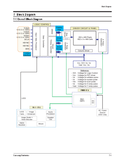
                                                                                                                                                          Block Diagram


7. Block Diagram
7-1 Overall Block Diagram
                          LOGIC CONTROL
             R-Data                                                                       Display
                                                                                                                 DRIVER CIRCUIT & PANEL


                                                                          DRAM
   8,10,12 or 13Bits                                                                       Data
            G-Data


                                                                                                    Driver
                          Input Data Processor


                                                                                                    Row
   8,10.12 or 13Bits
             B-Data


                                                    Data Controller
   8,10,12 or 13Bits                                                                                                      852 x 480 Pixels
                                                                                          Driver


                                                                                                                                                       Generator
             DCLK                                                                                                        852 x 3 x 480 Cells


                                                                                                                                                        X Pulse
                                                                      Timing Controller
                                                                                          Timing
           HSYNC


                                                                                                    Generator
                                                                                                     Y Pulse
                                                                           Driver
           HSYNC
                                                                                           Scan
              DEN                                                                         Timing
                                                                                                                          Column Driver
              LVDS
            Interface


                                                                                                                         Vcc 3V3 Va Vs
                                                                                                                          Vset Vsc Ve


                                                                                                                              Reference
                                                                                                                - 3V3    : Voltage for Logic Control
                                                                                                                - Vcc    : Voltage for FET driver
                                                                                                                - Va     : Voltage for address pulse
                                                                                                                - Vs     : Voltage for sustain pulse
                                                                                                                - Vsc    : Voltage for scan pulse
                                                                                                                - Ve     : Voltage for X ramp pulse
                                                                                                                - Vset   : Voltage for Y ramp pulse


         Image Scaler +
         Video Decoder

                                                 Micom


Samsung Electronics                                                                                                                                                7-1
Block Diagram


 CN804-1(Main SMPS)       CN803(Main SMPS)    CN810(Main SMPS)       CN2(DC-DC SMPS)    CN4(DC-DC SMPS)
                                                                                              
  CN102(Main Board)       CN101(Main Board)   CN2013(Logic Board)     CN5007(Y B'D)      CN4001(X B'D)
 Pin No.        Signal   Pin No.    Signal    Pin No.    Signal     Pin No.   Signal   Pin No.    Signal
      1          5.3V      1        6.5V        1        STBY         1        Vs         1       D5.3V
      2          RTN       2        RTN         2       VS_ON         2        Vs        2         Vg
      3          N/C       3         12V        3         N/C         3       RTN        3         RTN
      4          N/C       4        RTN         4       PS_ON         4       RTN        4         RTN
      5          RTN       5       18Vamp       5        RTN          5       Vset       5          Ve
      6          RTN       6       18Vamp       6        5.3V         6       RTN        6         RTN
      7          12V       7       RTN_amp      7        RTN          7       Vscan      7         RTN
      8         PS_ON      8       RTN_amp      8        RTN          8       RTN        8          Vs
      9          RTN       9         Vt         9        5.3V         9        Vg        9          Vs
      10         STBY      10       RTN         10       5.3V         10      D5.3V
      11        FAN_ON
      12        FAN_D

  CN6(DC-DC SMPS)
        
   CN2509(E-Buffer)
 Pin No.        Signal
      1          RTN
      2          N.C
      3         D5.3V
      4          N/C
      5           Va


7-2                                                                                      Samsung Electronics
                                                                                                                                           Block Diagram


7-2 Partial Block Diagram
7-2-1 Audio/Video Signal Block Diagram
                                                                       DDR (16MB )
                            RF Tu n er                                 K 4D263238D
                                                  SIF
                              A N A Tu n er                                                                Ren es as
                                                                                                            M30620
                            Vi d eo 1/2                                                                  Flash Memory
                                                                                                         144Pin
                                                                                                         16K RAM
                                                                       SVP PX
                                                                       (256-FPGA)
                            Si d e S.Vi d eo
                                                                       3D Comb                                EEPROM

                            Co m p o n en t 1/2                        Multi Decoder
                                                                       De-interlacer
                                                                                                                  L VDS
                                                                       Scaler                         LBE           Tx
                                                                       LVDS Out                       ( SD)       12b i t
                                                                       WXGA Output
                            PC
                                                                       DNIe (Demo)
                                                                       Caption/TTX2.5
                            HDMI                                       HDMI
                                                                       10b it p ro c ess


                                                                                                              H.P Am p
                            H.P                             Au d i o          A u d i o Pr o c es s           TDA7050
                                                            SW                    STV8257
                                                            HC4052            Lip Sync(120ms)             Au d i o A m p
                            Ser v i c e
                                                                                                           STA313W

                                                                                                                             10W

                                                            UA RT
                                                           MA X3223


7-2-2 DC-DC SMPS Block Diagram
                      Vs Input Part                                                                                         Vscan Output
                                                                                                Rectification
                                                                         Transformer
                                                                                                  Block


                                                                           Auxiliary
                                                   Control
                                                                            Power
                                                     and
                                               Switching Block                                    Feedback
                                                                                                    Block


                                                                                                                            Vset Output
                                                                                                Rectification
                                                                         Transformer
                                                                                                  Block


                                                   Control                 Auxiliary
                                                     and                    Power
                                               Switching Block                                    Feedback
                                                                                                    Block

                                                                                                                             Ve Output
                                                                                                Rectification
                                                                         Transformer
                                                                                                  Block


                                                   Control                 Auxiliary
                                                     and                    Power
                                               Switching Block                                    Feedback
                                                                                                    Block


Samsung Electronics                                                                                                                                 7-3
Block Diagram


7-2-3 Module Driver Board Block Diagram

1. Y Drive Board


2. X Drive Board


7-4                                       Samsung Electronics
                                                                                                                                Block Diagram


7-2-4 Logic Board Block Diagram
                                   30 Pin Connector          31 Pin LVDS          10 Pin (Power)           20 Pin Connector
                                Y-MAIN                 LVDS SIGNAL          RELAY_EINT              X-MAIN
                               CONTROL                   (8~12bit)            Vs-ON                CONTROL
                                SIGNAL                                                              SIGNAL

                              TX, RX
                              SCL, SDA
              5 Pin (uart)


                                         DRIVE     DDR                                                          DDR
                                                                           ASIC
                                         RESET     (FA)                                                         (MA)
                                                                                           DATA : 32bit
                                                                                           ADDR : 12bit
                                              DRIVE                                       DQS, CLK, nCLK
                                              nRESET


                              R,G,B : 24bit                                                          R,G,B : 24bit
                                CLK 1, 2                                                               CLK 1, 2
                             BLK, POC, STB                                                          BLK, POC, STB


                                   60 Pin Connector       FM75                                               60 Pin Connector


7-2-5 Powe Block Diagram


Samsung Electronics                                                                                                                      7-5
      MEMO


7-6          Samsung Electronics


◦ Jabse Service Manual Search 2024 ◦ Jabse PravopisonTap.bg ◦ Other service manual resources online : FixyaeServiceinfo