Service Manuals, User Guides, Schematic Diagrams or docs for : Samsung TV CL-29K5MQ Chassis K16A(N CL-29K5MQ 10_PCB Diagram
<< Back | HomeMost service manuals and schematics are PDF files, so You will need Adobre Acrobat Reader to view : Acrobat Download Some of the files are DjVu format. Readers and resources available here : DjVu Resources
For the compressed files, most common are zip and rar. Please, extract files with Your favorite compression software ( WinZip, WinRAR ... ) before viewing. If a document has multiple parts, You should download all, before extracting.
Good luck. Repair on Your own risk. Make sure You know what You are doing.
Image preview - the first page of the document
>> Download 10_PCB Diagram documenatation <<
Text preview - extract from the document
PCB Diagram
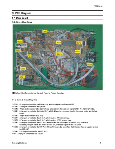
9. PCB Diagram
9-1 Main Board
9-1-1 Assy Main Board
CN601
CN503 CN900 CN702
CN902 CN701
CN501A
FN1
CN502
CN901
GT801
The Board that Controls Various Signals & Power for Product Operations
9-1-2 Names & Roles of Key Parts
* GT801 : A3 pin port connected to the Master Ass'y, which handles Master Power On/Off.
* CN601 : A4 pin port connected to the Speaker.
* CN902 : A4 pin port connected to the Control Ass'y, which delivers the necessary signal to KEY-IN1, KEY-IN2 Control.
* CN901 : A5 pin port connected to the Control Ass'y, which delivers the necessary signal to the remote control and the Led
control.
* CN602 : A5 pin port connected to AV Ass'y.
* CN701 : A8 pin port connected to the AV Ass'y, which receives AV2 external input.
* CN702 : A7 pin port connected to the AV Ass'y, which receives S-VHS external input.
* CN501 : A8 pin port connected to the CRT Ass'y which outputs the R/G/B signal to the CRT Ass'y for display.
In addition, this port outputs the necessary TILT, VM, and Power signals to the CRT Drive.
* CN502 : A6 pin port connected to the CRT Ass'y. Through this port, the power from the Deflection Block is supplied to drive
the CRT AMP.
* CN503 : A14 pin port connected to the CRT Ass'y.
* FN1 : A4 pin port connected to the Tilt Coil.
Samsung Electronics 9-1
PCB Diagram
9-1-3 Main Board Connector Pin
CN503 CN501A
Connected to the Main Ass'y Connected to the CRT Ass'y
PIN No. Pin Name PIN No. Pin Name
1 B-OUT 1 GND
2 G-OUT 2 N.C
3 R-OUT 3 GND
4 GND 4 HEATER
5 SENSE 5 N.C
6 GND 6 B+200V
7 N.C
8 GND
CN901
9 GND
Connected to the Control Ass'y
10 N.C
PIN No. Pin Name
11 GND
1 STD-LED
12 HEATER
2 TIME-LED
13 N.C
3 GND
14 B+200V
4 VCC
CN502
Connected to the CRT Ass'y
PIN No. Pin Name CN902
1 B-OUT Connected to the Control Ass'y
2 G-OUT PIN No. Pin Name
3 R-OUT 1 KEY-IN2
4 GND 2 KEY-IN1
5 SENSE 3 GND
6 GND 4 KEY-IN3
7 N.C
8 GND
CN701 CN900
Connected to the AV Ass'y Connected to Micom Jig
PIN No. Pin Name PIN No. Pin Name
1 AV2-R-IN 1 SCL
2 AV2-L-IN 2 GND
3 AV2-L-OUT 3 B+3.3V
4 AV2-R-OUT 4 SDA
5 GND
6 AV2-V-IN
7 GND
8 AV2-V-OUT
9-2 Samsung Electronics
PCB Diagram
CN702 CN601
Connected to the AV Ass'y Connected to the Speaker
PIN No. Pin Name PIN No. Pin Name
1 C-OUT 1 R+OUT
2 GND 2 R-OUT
3 Y-OUT 3 L+OUT
4 GND 4 L-OUT
5 C-IN
6 GND
7 Y-IN
FN01
Connected to the Tilt Coil
PIN No. Pin Name
1 TILT OUT
2 TILT OUT
3 GND
4 GND
Samsung Electronics 9-3
PCB Diagram
9-2 PIP Module
9-2-1 Assy PIP Module
9-2-2 Names & Roles of Key Parts
* CNP01 : A 12pin port inserted into the Main Ass'y, which connects various signal control ports necessary for PIP signal
processing and product operation.
* CNP02 : A 8pin port inserted into the Main Ass'y, which connects various signal control ports necessary for PIP signal
processing and product operation.
9-2-3 PIP Module Connector Pin
CNP01 CNP02
Connected to the Main Ass'y Connected to the Main Ass'y
PIN No. Pin NAME PIN No. Pin NAME
1 B+8V 1 OSD-R
2 B+5V 2 OSD-G
3 GND 3 OSD-B
4 SCL 4 OSD-F/B
5 SDA 5 SUb-CVBS
6 GND 6 GND
7 H-SYNC 7 PIP-CVBS
8 V-SYNC 8 C-IN
9 PIP-F/B
10 PIP-B
11 PIP-G
12 PIP-R
9-4 Samsung Electronics
PCB Diagram
9-3 CRT Board
9-3-1 Assy CRT Board
CN504
CN503
CN501,CN502,CN503
Through this port, the power from the DEFLECTION BLOCK & the R/G/B output signal from the Micom Module are supplied to
drive the CRT and AMP.
9-3-2 Names & Roles of Key Parts
* GT501, GT502, GT503 : The TBC-WIRE connection port. This port plays the role of the CRT Ground.
* CN503 : The R/G/B output signal from the Micom Module & the power, which is required to drive the CRT and the AMP, from the
Deflection Block is connected to this port.
9-3-3 CRT Board Connector Pin
CN503
Connects the R/G/B signal from the Micom Module
PIN No. Pin NAME
1 B-OUT
2 G-OUT
3 R-OUT
4 GND
5 SENSE
6 GND
7 N.C
8 GND
9 GND
10 N.C
11 GND
12 HEATER
13 N.C
14 B+200V
Samsung Electronics 9-5
MEMO
9-6 Samsung Electronics
◦ Jabse Service Manual Search 2026 ◦ Jabse Pravopis ◦ onTap.bg ◦ Other service manual resources online : Fixya ◦ eServiceinfo