Service Manuals, User Guides, Schematic Diagrams or docs for : Samsung Video DVD DVD-VR300 DVDVR300E_SB_1215146254
<< Back | HomeMost service manuals and schematics are PDF files, so You will need Adobre Acrobat Reader to view : Acrobat Download Some of the files are DjVu format. Readers and resources available here : DjVu Resources
For the compressed files, most common are zip and rar. Please, extract files with Your favorite compression software ( WinZip, WinRAR ... ) before viewing. If a document has multiple parts, You should download all, before extracting.
Good luck. Repair on Your own risk. Make sure You know what You are doing.
Image preview - the first page of the document
>> Download DVDVR300E_SB_1215146254 documenatation <<
Text preview - extract from the document
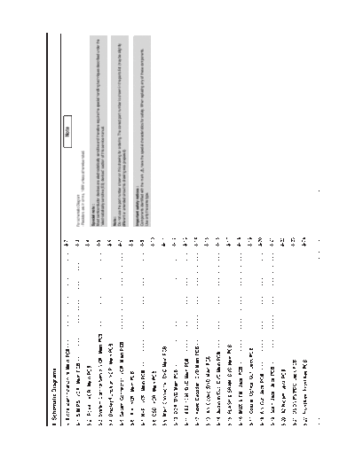
8. Schematic Diagrams

 Block Identification of Main PCB- - - - - - - - - - - - - - - - - - - - - - - - - - - - - - -           8-2                                                                          Note

8-1 S.M.P.S (VCR Main PCB)- - - - - - - - - - - - - - - - - - - - - - - - - - - - - - - - - - -          8-3          For schematic Diagram
                                                                                                                      - Resistors are in ohms, 1/8W unless otherwise noted.
8-2 Power (VCR Main PCB)- - - - - - - - - - - - - - - - - - - - - - - - - - - - - - - - - - - -          8-4
                                                                                                                       Special note :
8-3 System Control/Servo (VCR Main PCB) - - - - - - - - - - - - - - - - - - - - - - - - -                8-5           Most semiconductor devices are electrostatically sensitive and therefore require the special handling techniques described under the
                                                                                                                       "electrostatically sensitive (ES) devices" section of this service manual.

8-4 Display/Function (VCR Main PCB)- - - - - - - - - - - - - - - - - - - - - - - - - - - - -             8-6
                                                                                                                       Note :
                                                                                                         8-7           Do not use the part number shown on this drawing for ordering. The correct part number is shown in the parts list (may be slightly
8-5 Secam/Connector (VCR Main PCB) - - - - - - - - - - - - - - - - - - - - - - - - - - - -                            different or amended since this drawing was prepared).

8-6 A/V (VCR Main PCB)- - - - - - - - - - - - - - - - - - - - - - - - - - - - - - - - - - - - - -        8-8
                                                                                                                       Important safety notices :
8-7 Hi-Fi (VCR Main PCB) - - - - - - - - - - - - - - - - - - - - - - - - - - - - - - - - - - - - -       8-9           Components identified with the mark      have the special characteristics for safety. When replacing any of these components.
                                                                                                                       Use only the same type.

8-8 OSD (VCR Main PCB) - - - - - - - - - - - - - - - - - - - - - - - - - - - - - - - - - - - - -         8-10

8-9 Main Connector (DVD Main PCB) - - - - - - - - - - - - - - - - - - - - - - - - - - - - -              8-11

8-10 DDR (DVD Main PCB) - - - - - - - - - - - - - - - - - - - - - - - - - - - - - - - - - - - - -        8-12

8-11 IEEE 1394 (DVD Main PCB) - - - - - - - - - - - - - - - - - - - - - - - - - - - - - - - - -          8-13

8-12 Video Decoder (DVD Main PCB)- - - - - - - - - - - - - - - - - - - - - - - - - - - - - -             8-14

8-13 A/V Codec (DVD Main PCB)- - - - - - - - - - - - - - - - - - - - - - - - - - - - - - - - -           8-15

8-14 Audio In/Out (DVD Main PCB) - - - - - - - - - - - - - - - - - - - - - - - - - - - - - - -           8-16

8-15 FLASH & SRAM (DVD Main PCB) - - - - - - - - - - - - - - - - - - - - - - - - - - - - -               8-17

8-16 MUX & TM (Jack PCB) - - - - - - - - - - - - - - - - - - - - - - - - - - - - - - - - - - - -         8-18

8-17 Coaxlal/Optical Out (Jack PCB) - - - - - - - - - - - - - - - - - - - - - - - - - - - - - -          8-19

8-18 A/V Out (Jack PCB) - - - - - - - - - - - - - - - - - - - - - - - - - - - - - - - - - - - - - -      8-20

8-19 Scart Jack (Jack PCB) - - - - - - - - - - - - - - - - - - - - - - - - - - - - - - - - - - - -       8-21

8-20 A2/Nicam (Jack PCB) - - - - - - - - - - - - - - - - - - - - - - - - - - - - - - - - - - - - -       8-22

8-21 OSD/VPS/PDC (Jack PCB) - - - - - - - - - - - - - - - - - - - - - - - - - - - - - - - - - -          8-23

8-22 Front/Key (Front Key PCB) - - - - - - - - - - - - - - - - - - - - - - - - - - - - - - - - - -       8-24

Samsung Electronics                                                                  This Document can not be used without Samsung's authorization.                                                                                                           8-1
Schematic Diagrams


 Block Identification of Main PCB


         VCR MAIN PCB


8-2                                 This Document can not be used without Samsung's authorization.                      Samsung Electronics
                                                                                              Schematic Diagrams


8-1 S.M.P.S (VCR Main PCB)


Samsung Electronics          This Document can not be used without Samsung's authorization.                 8-3
Schematic Diagrams


8-2 Power (VCR Main PCB)


8-4                        This Document can not be used without Samsung's authorization.   Samsung Electronics
                                                                                                           Schematic Diagrams


8-3 System Control/Servo (VCR Main PCB)


Samsung Electronics                       This Document can not be used without Samsung's authorization.                 8-5
Schematic Diagrams


8-4 Display/Function (VCR Main PCB)


8-6                                   This Document can not be used without Samsung's authorization.   Samsung Electronics
                                                                                                      Schematic Diagrams


8-5 Secam/Connector (VCR Main PCB)


Samsung Electronics                  This Document can not be used without Samsung's authorization.                 8-7
Schematic Diagrams


8-6 A/V (VCR Main PCB)


8-8                      This Document can not be used without Samsung's authorization.   Samsung Electronics
                                                                                            Schematic Diagrams


8-7 Hi-Fi (VCR Main PCB)


Samsung Electronics        This Document can not be used without Samsung's authorization.                 8-9
Schematic Diagrams


8-8 OSD (VCR Main PCB)


8-10                     This Document can not be used without Samsung's authorization.   Samsung Electronics
                                                                                                     Schematic Diagrams


8-9 Main Connector (DVD Main PCB)


Samsung Electronics                 This Document can not be used without Samsung's authorization.                8-11
Schematic Diagrams


8-10 DDR (DVD Main PCB)


8-12                      This Document can not be used without Samsung's authorization.   Samsung Electronics
                                                                                                 Schematic Diagrams


8-11 IEEE 1394 (DVD Main PCB)


Samsung Electronics             This Document can not be used without Samsung's authorization.                8-13
Schematic Diagrams


8-12 Video Decoder (DVD Main PCB)


8-14                                This Document can not be used without Samsung's authorization.   Samsung Electronics
                                                                                                 Schematic Diagrams


8-13 A/V Codec (DVD Main PCB)


Samsung Electronics             This Document can not be used without Samsung's authorization.                8-15
Schematic Diagrams


8-14 Audio In/Out (DVD Main PCB)


8-16                               This Document can not be used without Samsung's authorization.   Samsung Electronics
                                                                                                    Schematic Diagrams


8-15 FLASH & SRAM (DVD Main PCB)


Samsung Electronics                This Document can not be used without Samsung's authorization.                8-17
Schematic Diagrams


8-16 MUX & TM (Jack PCB)


8-18                       This Document can not be used without Samsung's authorization.   Samsung Electronics
                                                                                                       Schematic Diagrams


8-17 Coaxlal/Optical Out (Jack PCB)


Samsung Electronics                   This Document can not be used without Samsung's authorization.                8-19
Schematic Diagrams


8-18 A/V Out (Jack PCB)


8-20                      This Document can not be used without Samsung's authorization.   Samsung Electronics
                                                                                              Schematic Diagrams


8-19 Scart Jack (Jack PCB)


Samsung Electronics          This Document can not be used without Samsung's authorization.                8-21
Schematic Diagrams


8-20 A2/Nicam (Jack PCB)


8-22                       This Document can not be used without Samsung's authorization.   Samsung Electronics
                                                                                               Schematic Diagrams


8-21 OSD/VPS/PDC (Jack PCB)


Samsung Electronics           This Document can not be used without Samsung's authorization.                8-23
Schematic Diagrams


8-22 Front/Key (Front PCB)


8-24                         This Document can not be used without Samsung's authorization.   Samsung Electronics
◦ Jabse Service Manual Search 2026 ◦ Jabse Pravopis ◦ onTap.bg ◦ Other service manual resources online : Fixya ◦ eServiceinfo