Service Manuals, User Guides, Schematic Diagrams or docs for : TOSHIBA DVD SD-110 sd-110e_schematics

<< Back | Home

Most service manuals and schematics are PDF files, so You will need Adobre Acrobat Reader to view : Acrobat Download Some of the files are DjVu format. Readers and resources available here : DjVu Resources
For the compressed files, most common are zip and rar. Please, extract files with Your favorite compression software ( WinZip, WinRAR ... ) before viewing. If a document has multiple parts, You should download all, before extracting.
Good luck. Repair on Your own risk. Make sure You know what You are doing.


Image preview - the first page of the document
sd-110e_schematics


>> Download sd-110e_schematics documenatation <<

Text preview - extract from the document
5-3. Main Circuit Diagrams
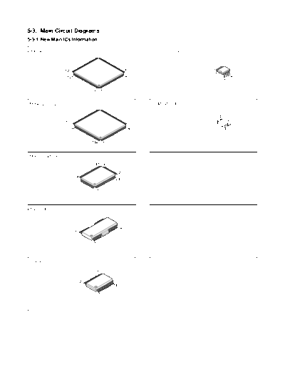
5-3-1. New Main ICs Information

ZR36732                                                            TA1319P/TA1319AP
                                     81 80

                                                                                            5
                                                             41                         8
                   120
                    121                                      40                                     4
                                                                                                1

                                    160 1


TMP94C251AF(Z)                                                     S-814A50AUC-BDO-T2
                                     73       72

                                                                                            4
                   108                                        37                        5
                                                                                                    3
                    109                                       36                                1


                                    144       1


TMP87CH74AF-2C07

                                      41      40

                                                        25
                          64
                                                    24
                          65

                                    80 1


BA5813FM-E2
                                           15


                                                        14
                          28


                                     1


AD1959YRSRL

                                         15

                               28
                                                   14

                                          1
5-3-2. Main Circuit Diagram


                              Fig. 3-5-5
Main Circuit Diagram                                                   Output-RGB Circuit Diagram

 1 J301 Composite            E-7   4 J301 L ch output            E-7    6 JV01 SCART output                    C-10
          video output                     / R ch output         E-7       (Video out select : RGB)
                                             (1 kHz, FS)

                                                                                        NTSC 100% color bar (Play)
                                                                                        75 terminated


                 CVBS output                                                                            V: 1 V/div
                                                                                      (a) Pin 19 : CV
                 75W terminated                    L ch output                                          H: 20 


◦ Jabse Service Manual Search 2024 ◦ Jabse PravopisonTap.bg ◦ Other service manual resources online : FixyaeServiceinfo