Service Manuals, User Guides, Schematic Diagrams or docs for : Yamaha RX RX-A3010 & V3071 RXA3010_DISPLAY
<< Back | HomeMost service manuals and schematics are PDF files, so You will need Adobre Acrobat Reader to view : Acrobat Download Some of the files are DjVu format. Readers and resources available here : DjVu Resources
For the compressed files, most common are zip and rar. Please, extract files with Your favorite compression software ( WinZip, WinRAR ... ) before viewing. If a document has multiple parts, You should download all, before extracting.
Good luck. Repair on Your own risk. Make sure You know what You are doing.
Image preview - the first page of the document
>> Download RXA3010_DISPLAY documenatation <<
Text preview - extract from the document
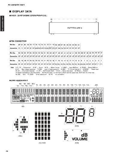
                         RX-A3010/RX-V3071


                           DISPLAY DATA
                           V4001 : 23-MT-04GINK (OPERATION P.C.B.)
RX-A3010/RX-V3071


                                                                                                                                82                                                                                           1


                                                                                                                                                              PATTERN AREA


                           PIN CONNECTION

                          Pin No.         82 81 80 79 78 77 76 75 74 73 72 71 70 69 68 67 66 65 64 63 62 61
                          Connection F2 F2 NP NP NP NP LGND PGND VH VDD OSC RESET CS CP DA TSA TSB NP NP NP NP NP

                          Pin No.         60 59 58 57 56 55 54 53 52 51 50 49 48 47 46 45 44 43 42 41 40 39 38 37 36 35 34 33 32 31
                          Connection NP NP NP NP NP NP NP NP NP NP NP NP NP NP NP NP NP NP NP NP NP NP NP NP NP NP NP NP NP NP

                          Pin No.         30 29 28 27 26 25 24 23 22 21 20 19 18 17 16 15 14 13 12 11 10 9                                                                                         8      7   6     5    4   3     2   1
                          Connection NP NP NP NP NP NP NP NP NP NP NP NP NP NC NC NC NC NC NC NC NC NC Q23G 23G NP NP NP NP F1 F1
                           Note : 1) F1, F2 ..... Filament pin 2) NP ..... No pin 3) DL ..... Datum line pin 4) LGND ..... Logic GND pin 5) PGND ..... Power GND pin
                                  6) HV ..... High voltage supply pin 7) VDD ..... Logic voltage supply pin 8) OSC ..... Pin for self-oscillation 9) RESET ..... Reset input
                                  10) CS ..... Chip select input pin 11) CP ..... Shift resister clock 12) DA ..... Serial data input 13) TSA,B ..... Test pin
                                  14) Solder composition is Sn-3Ag-0.5Cu. 15) Field of vision is a minimum of 25.0
◦ Jabse Service Manual Search 2026 ◦ Jabse Pravopis ◦ onTap.bg ◦ Other service manual resources online : Fixya ◦ eServiceinfo