Service Manuals, User Guides, Schematic Diagrams or docs for : Yamaha RX RX-A3010 & V3071 SCHE_PRINT_RXA3010_RXV3071_DIGI1_2

<< Back | Home

Most service manuals and schematics are PDF files, so You will need Adobre Acrobat Reader to view : Acrobat Download Some of the files are DjVu format. Readers and resources available here : DjVu Resources
For the compressed files, most common are zip and rar. Please, extract files with Your favorite compression software ( WinZip, WinRAR ... ) before viewing. If a document has multiple parts, You should download all, before extracting.
Good luck. Repair on Your own risk. Make sure You know what You are doing.


Image preview - the first page of the document
SCHE_PRINT_RXA3010_RXV3071_DIGI1_2


>> Download SCHE_PRINT_RXA3010_RXV3071_DIGI1_2 documenatation <<

Text preview - extract from the document
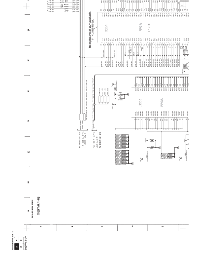
RX-A3010/RX-V3071

  A     B

  C     D

DIGITAL1 4/9
                                A              B   C                     D          E   F                G                   H
                           RX-A3010/RX-V3071


                             DIGITAL1 4/9
                    1
                    CB23


                    2


                                                       to DIGITAL1 1/9


                                                                                            No replacement part available.


                                                       to DIGITAL1 3/9
                    3
                                                                                                         IC51


                    4


                                                                             IC51                        FPGA


                    5                                                        FPGA
                                                                                    RX-A3010/RX-V3071

                                                                                            A    B

                                                                                            C    D

                                                                                        DIGITAL1 4/9
     H       I                       J    K   L              M                  N


                                                  to DIGITAL1 5/9


         No replacement part available.
e.
                                                              to DIGITAL1 6/9


                      IC51


                     FPGA
                    6


                    7


                    8                                   No replacement part available.
                               CB52


                                                                                         to DIGITAL1 6/9   to DIGITAL1 7/9

                    9

                                                                                                                             IC52: M12L128168A-5TG2L
                                      to DIGITAL1 6/9                                                                        2 M x 16-bit x 4 banks synchronous DRAM

                                                                                                                             CLK       Clock
                                                                                                                                       Generator
                                                                                                                             CKE


                                                                                                                             Address                                              Row
                                                                                                                                                                                  Address
                                                                                                                                                                                  Buffer
                                                                                                                                                                 Mode             and
                                                                                                                                                                 Register         Refresh
                                                                                                                                                                                  Counter


                    10


                                                                                                                                               Command Decoder
                                                                                                                             CS                                                   Column


                                                                                                                                                                  Control Logic
                                                                                                                                                                                  Address
                                                                                                                             RAS
                                                                                                                                                                                  Buffer
                                                                                                                             CAS                                                  and
                                                                                                                                                                                  Counter
                                                                                                                             WE


                         130


RX-A3010/RX-V3071

  A     B

  C     D

DIGITAL1 4/9
                                                                                                                                                                                                                                                                                  to DIGITAL1 2/9


                                                                                                                                                                        IC53


                                                                                                                                                                                                                                             IC54


                                                                                                                                                                 IC53


                                                    SDRAM 128 Mbit
                                                                                                      IC52


                                                                                                                                                                                                                                   DIGITAL1 (1)


                                                                                                                                                                               IC54: R1172H121D-T1-F
                                                                                                                                                                               CMOS-based positive-voltage regulator IC

                                                                                                                                IC53: TC7SH125FU
                                                                                                                                                                               VDD 4                            5 VOUT
onous DRAM                                                                                      VDD    1     54   VSS           Bus buffer
                                                                                               DQ0     2     53   DQ15
                                                                                              VDDQ     3     52   VSSQ                                                                                                   Pin No.    Symbol               Description
                                                                                               DQ1     4     51   DQ14                                                                                                     1          CE        Chip Enable Pin
                                         Bank D
                                                                                               DQ2     5     50   DQ13           G    1              5 VCC
                                                                                                                                                                                         Vref
                                                                                                                                                                                                                            2        GND        Ground Pin
                                                                                               VSSQ    6     49   VDDQ
                                       Bank C                                                                                                                                                                              3         NC         No Connection
                                                                                               DQ3     7     48   DQ12                                                                          Current Limit
                                     Bank B
     Row
                                                                                               DQ4     8     47   DQ11        IN A    2                                        CE 1                             2 GND      4         VDD        Input Pin
                                                                                              VDDQ     9     46   VSSQ                                                                                                     5         VOUT       Output Pin of Voltage Regulator
               Row Decoder


     Address
                                                                                               DQ5     10    45   DQ10
     Buffer
                                   Bank A                                                      DQ6     11    44   DQ9         GND 3                 4   OUT Y
     and
                                                                                               VSSQ    12    43   VDDQ
     Refresh
                                                                                               DQ7     13    42   DQ8
     Counter
                                                                                                VDD    14    41   VSS
                                                                                             LDQM      15    40   NC
                               Sense Amplifier                                                  WE     16    39   UDQM
                                                                           L(U)DQM             CAS     17    38   CLK
     Column                   Column Decoder                                                   RAS     18    37   CKE
     Address                                                                                     CS    19    36   NC
                                                                     Input and Output


     Buffer                                                                                    BA0     20    35   A11
                                                     Latch Circuit


     and                                                                                       BA1     21    34   A9      Components having special characteristics are marked         and must be replaced
                                                                          Buffer


                                                                                             A10/AP    22    33   A8
     Counter                 Data Control Circuit                                       DQ       A0    23    32   A7
                                                                                                                          with parts having specifications equal to those originally installed.
                                                                                                 A1    24    31   A6      Schematic diagram is subject to change without notice.
                                                                                                 A2    25    30   A5
                                                                                                 A3    26    29   A4
                                                                                                VDD    27    28   VSS


                                                                                                                                                                                                                                                                                                    RX-A3010/RX-V3071

                                                                                                                                                                                                                                                                                                            A    B

                                                                                                                                                                                                                                                                                                            C    D

                                                                                                                                                                                                                                                                                                        DIGITAL1 4/9
RX-A3010/RX-V3071

  A     B

  C     D

DIGITAL1 5/9
                          A            B          C              D   E          F                 G


                        DIGITAL1 5/9
                    1                                 HDMI OUT
                                                         1
                                                        ARC
                                           CB61


                    2


                                                                                    IC68


                    3


                                                                                           IC67


                    4
                                                                         IC65


                    5
                                                                          RX-A3010/RX-V3071

                                                                                  A    B

                                                                                  C    D

                                                                              DIGITAL1 5/9
G          H              I   J      K   L   M                     N
                                                      RX-A3010/RX-V3071


               HDMI OUT
                  2

    CB62


                              IC66


                                                 to DIGITAL1 1/9


                                                 to DIGITAL1 6/9
                    6    HDMI TRANSMITTER

                              IC61


                    7


                    8


                    9                  IC61, 62: SiI9134CTU
                                       HDMI transmitter             INT HPD

                                                                                                                                                        IC64: TC74LC
                                     RESET#                                                                                                             Low voltage oc
                                       CSDA                                                                                                             with 5-V tolera
                                                     CI2CA                                                     DSCL
                                       CSCL          Slave                                           E-DDC
                                                                   Registers                         Master    DSDA                                      DIR   1
                                     VSYNC                            and
                                                      Video       Configuration         HDCP                                                              A1   2
                                     HSYNC            Data                            Encryption   HDCP Keys               IC63: TC74VHC157FT
                                       IDCK                          Logic                          EEPROM
                                                     Capture                           Engine                              Quad 2-channel multiplexer     A2   3
                                         DE         Logic/DE
                                     D[35:0]        Generator                                                  EXT_SWING   SELECT 1            16 Vcc     A3   4

                                                                                                                               1A 2    ASG     15 ST      A4   5
                                                                    YCbCr to RGB                                               1B 3    B   A   14 4A
                    10                                               Color Space         XOR       HDMI 1.3
                                                                                                                Tx0            1Y 4    Y   B   13 4B
                                                                                                                                                          A5   6

                                     S/PDIF                           Converter/         Mask                   Tx1            2A 5            12 4Y      A6
                                                                                                    TMDS                               A   Y                   7
                                      MCLK                           4:2:2 to 4:4:4                             Tx2
                                                                                                     Core                      2B 6    B   A   11 3A
                                        WS                             Converter                                TxC                                       A7   8
                                                         Audio                                                                 2Y 7    YYB     10 3B
                                       SCK              Capture                                                              GND 8             9   3Y     A8   9
                                     SD[3:0]             Logic
                                     DL[3:0]                                                                                                             GND 10
                                     DR[3:0]


RX-A3010/RX-V3071

  A     B

  C     D

DIGITAL1 5/9
                 HDMI TRANSMITTER

                                     IC62
                                                                                                                                              IC64
                                                                                                                                                                                                   to DIGITAL1 9/9


                                                                                                      IC63


                                                                                                                                                                                                   to DIGITAL1 4/9


IC64: TC74LCX245FT                          IC65, 66: NJM2888F05
Low voltage octal bus transceiver           Low dropout voltage regulator
with 5-V tolerant inputs and outputs
                                                                                                                                                                                           DIGITAL1 (1)

 DIR   1                  20   Vcc                                                                           IC68: TC7WHU04FU
                                               VIN 5                                         4 VOUT          Triple inverter
  A1   2                  19   OE

  A2   3                  18   B1           Control 1                            Thermal                         VCC   1Y   3A   2Y

  A3   4                  17   B2                                               Protection                        8    7    6     5

  A4   5                  16   B3                                   Bandgap
                                                                    Reference                                                           Components having special characteristics are marked         and must be replaced
  A5   6                  15   B4                                                                                                       with parts having specifications equal to those originally installed.
  A6   7                  14   B5                                                                                                       Schematic diagram is subject to change without notice.
  A7   8                  13   B6
                                                                                                                  1    2    3     4
  A8   9                  12   B7                                                                                 1A   3Y   2A   GND

 GND 10                   11   B8
                                              GND 2


                                                                                                                                                                                                                            131


                                                                                                                                                                                                                                  RX-A3010/RX-V3071

                                                                                                                                                                                                                                          A    B

                                                                                                                                                                                                                                          C    D

                                                                                                                                                                                                                                      DIGITAL1 5/9
RX-A3010/RX-V3071

  A     B

  C     D

DIGITAL1 6/9
                             A                   B          C          D          E             F                                 G                                                H
                        RX-A3010/RX-V3071


                          DIGITAL1 6/9
                    1                                                                               to DIGITAL1 1/9      to DIGITAL1 2/9     to DIGITAL1 3/9   to DIGITAL1 4/9   to D


                                                     IC87


                                                                           IC85
                    2


                                                                                      IC80
                                                                                         IC80


                                                                                         IC80


                                                     IC86


                                                                           IC84
                    3

                               to DIGITAL1 3/9


                                                                IC82


                    4


                                                                                                                      MICROPROCESSOR

                    5
                                                                                                                                      IC81


                                                                                                                  No replacement part available.
                                                                                                                                                                                                                                                                                                   RX-A3010/RX-V3071

                                                                                                                                                                                                                                                                                                           A    B

                                                                                                                                                                                                                                                                                                           C    D

                                                                                                                                                                                                                                                                                                       DIGITAL1 6/9
                   H                                 I                     J   K                                              L                                     M                                                                                                N


o DIGITAL1 4/9   to DIGITAL1 5/9   to DIGITAL1 8/9       to DIGITAL1 7/9
                                                                                   to DIGITAL1 9/9


                                                                                                                                                                                 IC80, 96: TC7WZ32FK (TE85L, F)
                                                                                                                                                                                 Dual 2-input OR gate


                                                                                                                                                                                    1A 1                                                               8 Vcc

                                                                                                                                                                                    1B 2                                                               7 1Y

                                                                                                                                                                                    2Y 3                                                               6 2B

                                                                                                                                                                                GND 4                                                                  5 2A


                                                                                                                                          IC81: R5F6416MADFE
                                                                                                                                          Single chip 32-bit microprocessor
                                                                                                                                                   8               8                8                 8                        8               8                 8             8


                                                                                                                                              Port P0         Port P1          Port P2         Port P3         Port P4                    Port P5        Port P6          Port P7


                                                                                                                                                                                                                                                                                    Port P8
                                                                                                                                                         Peripheral functions
                                                                                                                                                                                                   A/D converter:                               Clock generator:


                                                                                                                                                                                                                                                                                               7
                                                                                                                                                                Timer:
                                                                                                                                                    Timer A16 bits 


◦ Jabse Service Manual Search 2024 ◦ Jabse PravopisonTap.bg ◦ Other service manual resources online : FixyaeServiceinfo