Service Manuals, User Guides, Schematic Diagrams or docs for : motorola MMS1117_128K_Unibus_Memory_Sep78
<< Back | HomeMost service manuals and schematics are PDF files, so You will need Adobre Acrobat Reader to view : Acrobat Download Some of the files are DjVu format. Readers and resources available here : DjVu Resources
For the compressed files, most common are zip and rar. Please, extract files with Your favorite compression software ( WinZip, WinRAR ... ) before viewing. If a document has multiple parts, You should download all, before extracting.
Good luck. Repair on Your own risk. Make sure You know what You are doing.
Image preview - the first page of the document
>> Download MMS1117_128K_Unibus_Memory_Sep78 documenatation <<
Text preview - extract from the document
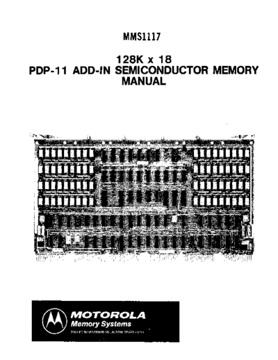
             MMSll17

              128K x 18
PDP-11 ADD-IN SEMICONDUCTOR MEMORY
               MANUAL
            MMSll17


       USER MANUAL


PRODUCT:      MMSll17 Family
              Artwork Revisions A and B
DOCUMENT:     Edition A
              Revision 2


                                  1 September 78
                               TABLE OF CONTENTS

PARAGRAPH
            CHAPTER I.     SPECIFICATIONS
1.0         Introduction
1.1         Option Designations
1.2         Pinout
1.3         Physical
1.4         Environmental Requirements
1.5         Compatibility
1.6         Storage Capacity
1.7         Bus Loading
1.8         Addressing
1.9         I/O Page Use As R/W Memory
1.10        Parity
1.11        Timing
1.12        Refresh Latency
1.13        Power Requirements
            CHAPTER II:    THEORY OF OPERATION
            CHAPTER III:     INSTALLATION
3.1         MMSll17 xxPC, Using the Internal Parity Controller
3.2         MMSll17 xxP (and MMSlll7 xxPC) Using External Parity Generator
3.3         MMSll17xx No Parity
3.4         Battery Backup Mode, All Modules
            CHAPTER IV:     REPAIR AND WARRANTY


                                       i
                              CHAPTER I.   SPECIFICATIONS


1.0          INTRODUCTION
                 This manual describes the specifications, installation and
             operation of the MMSll17 memory system.
                 The MMSll17 is a family of single-card memory systems, designed
             for, and fully compatfble with, PDP-ll* Unibus* mini-computers.
                 It is capable of storing up to 128 kilobytes of data on a
             single hex-height module. Parity storage as well as controller
             functions are optionally available on the same module.
                 The power and signal pin-outs are compatible with any hex-SPC
             slot and thus obviate the need for a specific memory back panel.

1.1          OPTION DESIGNATIONS
                 The several available options are designated with a 4 character
             suffix to the basic name as shown in the following table:
                     TABLE 1: MMSll17 OPTION DESIGNATOR SUFFIX

      Typical
      Read
      Access      Pari ty Opt; ons:             Total Storage Capacity (in kilobytes)
      Time                                      32K B      64K C:>    96K ()    128KB
      290 nsec    parity + controller           -32-PC      -34-PC    -36-PC     -38-PC
                  parity data only              -32-P       -34-P     -36-P      -38-P
                  no pari ty                    -32         -34       -36        -38

      360 nsec    parity + controller           -42-PC      -44-PC    -46-PC     -48-PC
                  pari ty data only             -42-P       -44-P     -46-P      -48-P
                  no parity                     -42         -44       -46        -48
  I
  1390 nsec       parity + controller           -52-PC      -54-PC    -56-PC     -58-PC
  1               parity data only              -52-P       -54-P     -56-P      -58-P
  1               no parity                     -52         -54       -56        -58
  1


*Trademark of Digital Equipment Corp.


                                           1
SPECIFICATIONS (contld)
1.2   PINOUT
           All electrical signal connections to the system are made to the
      UNIBUS* pins available at the Small Peripheral Controller (SPC)
      connectors (i .e., connector row C, D, E and F).
                        TABLE 2:     MMSll17 CONNECTOR PINOUT
           SIGNAL                  PIN                 SIGNAL         PIN
           A 00 L                  EH2                 D 06 L         CV2
           A 01 L                  EH1                 D 07 L         CM2
           A 02 L                  EF1                 D 08 L         CL2
           A 03 L                  EV2                 D 09 L         CK2
           A 04 L                  EU2                 D 10 L         CJ2
           A 05 L                  EV1                 D 11 L         CH1
           A 06 L                  EU1                 D 12 L         CH2
           A 07 L                  EP2                 D 13 L         CF2
           A 08 L                  EN2                 D 14 L         CE2
           A 09 L                  ER1                 D 15 L         CD2
           A 10 L                  EP1
           A 11 L                  ELl                 DCLO L         CN1
           A 12 L                  EC1                 INIT L         DLl
           A 13 L                  EK2                 MSYN L         EEl
           A 14 L                  EK1                 NPG IN         CAl
           A 15 L                  ED2                 NPG OUT        CBl
           A 16 L                  EE2                 PA L           CCl
           A 17 L                  ED1                 PB L           CSl
                                                      *PAR DET        BE2
           BG   4 IN               DS2
           BG   4 OUT              DT2                *PO L           AP1
           BG   5 IN               DP2                *P1   L         AN1
           BG   5 OUT              DR2                 SSYN L         EJ1
           BG   6 IN               DM2                *SSYN INT. L    BEl
           BG   6 OUT              DN2
           BG   7 IN               DK2                 +5    VDC      DA2, EA2
           BG   7 OUT              DL2                                FA2
                                                       +5       SB    BD1
           CO     l                EJ2                 -15      VDC   FB2
           Cl     L                EF2
                                                       +20      VDC   AR1, AV1
           D 00 L                  CS2                                CE1, CU1
           D 01 L                  CR2
           D 02 L                  CU2                 GND            AC2, ATl
           D 03 L                  CT2                                BC2, Bn
           D 04 L                  CN2                                CC2
           D 05 L                  CP2                                DC2, DTl
                                                                      EC2, FTl

*These signals are used only when the MMSll17-XX-PC and MMSll17-XXP models are
used in conjunction with an external parity control module. This configuration
is available in certain "Modified Unibus" backpanels.

                                         2
SPECIFICATIONS (cont'd)
1.3    PHYSICAL
            The MMS1l17 is imp1 emented o.n one standard "Hex-hei ght" pri nted
       circuit card, compatible with all PDP-ll* backpanel connectors and
       card cages; it requires only one single (1/2") width connector slot.
1 .4   ENVIRONMENTAL REQUIREMENTS
            Storage Temperature Range:       o to   70 degrees C.
            Operating Temperature Range:     o to   70 degrees C.
            Relative Humidity:               o to   90 percent without condensation
1.5    COMPATIBILITY
            The MMS1l17 interfaces electrically with the PDP-l1* UNIBUS* as
       well as the newer modified Unibus* and is logically as well as
       electrically compatible with the AC and DC parameters specified by it.
1.6    STORAGE CAPACITY
             Fully populated capacity is 128 kilobytes; optional 96, 64 or 32
       ki 1obytes.

1.7    BUS LOADING
            The MMSl17 presents one standard bus load to the UNIBUS*.
       This parameter is independent of the memory size or parity options
       selected.

1.8    ADDRESSING
             The MMS1l17 interfaces to all 18 bus address lines. The memory's
       starting address can be selected via switches located in position U58,
       to fallon any 4K word boundary between 0 and l12K. In addition, 1 or
       2 ki10words of the I/O page (at address l24K to l26K) can selectively
       be made available for random access storage. See Table 3 for specific
       selections.


                                      3
                                TABLE 3:   MMSll17 STARTING ADDRESS SELECTION

                              STARTING             SWITCH POSITION (X     = closed, o = open)
                      ADDRESS       BANK NO.           U58/5   U58/4    U58/3   U58/2    U58/1
                        OK              0                a       0        0       0        0
                        4K              1                0       0        0       0          X
                        8K              2                0       0        0        x         0
                       12K              3                0       0        0        x         X
                       16K              4                0       0        x       0          0
                       20K              5                0       0        X       0          X
                       24K              6                0       0        x        x         0
                       28K              7                0       0        x       X          X
                       32K              8                0       X        0       0          0
                       36K              9                a       X        0       0          X
                       40K             10                0       X        a       X          0
                       44K             11                a       x        a        x         x
                       48K             12                a       x        x        0         a
                       52K             13                a       x        x       a          X
                       56K             14                a       x        X       x          a
        x~
◦ Jabse Service Manual Search 2024 ◦ Jabse Pravopis ◦ onTap.bg ◦ Other service manual resources online : Fixya ◦ eServiceinfo