Service Manuals, User Guides, Schematic Diagrams or docs for : motorola Mobile Phone W215_W218_sm W215_W218_Circuit_Description
<< Back | HomeMost service manuals and schematics are PDF files, so You will need Adobre Acrobat Reader to view : Acrobat Download Some of the files are DjVu format. Readers and resources available here : DjVu Resources
For the compressed files, most common are zip and rar. Please, extract files with Your favorite compression software ( WinZip, WinRAR ... ) before viewing. If a document has multiple parts, You should download all, before extracting.
Good luck. Repair on Your own risk. Make sure You know what You are doing.
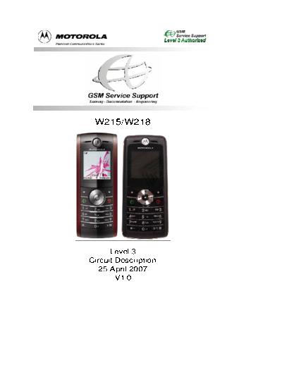
Image preview - the first page of the document

>> Download W215_W218_Circuit_Description documenatation <<
Text preview - extract from the document
 W215/W218


      Level 3
Circuit Description
   25 April 2007
        V1.0
W215/W218 Level 3 C


 Index
1     Receive .................................................................................................... 4
    1.1    Band selection........................................................................................... 4
    1.2    Demodulation............................................................................................ 5
    1.3    Audio Codec.............................................................................................. 6
      1.3.1 Voice Downlink Patch..................................................................................................7
    1.4    Earpiece Receiver ...................................................................................... 7
    1.5    Headset .................................................................................................... 7
    1.6    Speaker Phone .......................................................................................... 7
    1.7    Data Download Receive Path ...................................................................... 8

2     Transmit .................................................................................................. 8
    2.1    Audio (Voice uplink Patch).......................................................................... 9
    2.2    Data Download Transmit Path .................................................................... 9
    2.3    Stereo Audio Path...................................................................................... 9
    2.4    Modulation................................................................................................................... 10
    2.5    RF TX PA ............................................................................................... 12
    2.6    TX PA Power Control in SKY77318 .......................................................... 13

3     Triton-Lite Monitoring ADC ....................................................................14

4     Baseband Serial Port (BSP) ....................................................................15

5     Microcontroller Serial Port (USP) ...........................................................15

6     General purposes I/O (GPIO).................................................................15

7     TFT LCD Display......................................................................................17
    7.1    Display Backlights ...................................................................................................... 18
    7.2 Image Processor ...................................................................................... 18
    7.3 Camera Module ........................................................................................ 19

8     32kHz RTC ..............................................................................................19

9     SIM Card Circuit .....................................................................................19
    9.1    SIM Card Supply Voltage Generation ......................................................... 20

10 Keypad................................................................................................... 20
    10.1 Keypad Matrix ......................................................................................... 21

11 Vibrator circuit .......................................................................................21

                                               Motorola Proprietary Information
                                                                  -2-
W215/W218 Level 3 C
12 Memory ..................................................................................................21

13 Power .....................................................................................................22
  13.1 Low-Dropout Voltage Regulators............................................................... 22
  13.2 Power Down Methods .............................................................................. 23

14 Sleep Module ..........................................................................................23
  14.1 Sleep Up Sequence.................................................................................. 24
  14.2 Sleep off Sequence .................................................................................. 24

15 Power Tree .............................................................................................25

16 Charging Circuit and External Power .....................................................25
  16.1 Battery Support ....................................................................................... 25
  16.2 Charger Support...................................................................................... 25


                                       Motorola Proprietary Information
                                                      -3-
W215/W218 Level 3 C
1 Receive

1.1   Band selection
     The radio frequency signal is received from internal PIFA-type antenna. Received
GSM RF signal enters to PCB through the RF switch JP201. At this moment the T/R switch
SW201 is switched to RX mode to let the signal input to next stage. Then the signal goes
into SAW filter, BF201 and BF202 , which reject out-band signal and transfer the signal
from single-end to balanced. And the matching circuits between T/R switch and SAW
filter reduce the unwanted RF signal reflection and provide a flat frequency response in the
operation band. Finally the received signal will fed into Locosto Plus U101 DRP core
through a balanced MLCC matching network. The following table describes the control
voltages of T/R switch and PA:
                         SW_LO_TX SW_HI_TX                        VAPC
                                                         PA_EN             BS1
            W215            PIN 5           PIN 2                 PIN 20
                                                          TP201           TP202
                           of T201         of T201                of U201
            Standby          Low               x           Low     Low        x
         RX EGSM900          Low             Low           Low     Low       Low
         RX DCS1800          Low             Low           Low     Low      High
          TX GSM900          High            High          High    High      Low
         TX DCS1800          High            High          High    High     High


   The RF signal is received by internal antenna or by RF plug, and the signal is passing
through the RF switch JP201 and then fed into T/R switch. The low band (GSM900) RX
received signal is transmitted from SW201 (Pin 11) and input to low-band SAW filter
BF201, while the high band (DCS1800) RX received signal from SW201 (Pin 1) and then
input to high-band SAW filter BF202. The last stage of RX on PCB is Locosto U101
(Loocsto-Plus), and the DRP process will make the signal into binary data.


                       Figure 1: Locosto TX/RX Paths Description

                               Motorola Proprietary Information
                                            -4-
W215/W218 Level 3 C

1.2   Locosto RX Mode                                                                           Formatiert: Nummerierung
                                                                                                und Aufz
◦ Jabse Service Manual Search 2024 ◦ Jabse Pravopis ◦ onTap.bg ◦ Other service manual resources online : Fixya ◦ eServiceinfo