Service Manuals, User Guides, Schematic Diagrams or docs for : acer Acer Aspire 4315_4715_Wistron_Volvi2_Rev-1

<< Back | Home

Most service manuals and schematics are PDF files, so You will need Adobre Acrobat Reader to view : Acrobat Download Some of the files are DjVu format. Readers and resources available here : DjVu Resources
For the compressed files, most common are zip and rar. Please, extract files with Your favorite compression software ( WinZip, WinRAR ... ) before viewing. If a document has multiple parts, You should download all, before extracting.
Good luck. Repair on Your own risk. Make sure You know what You are doing.


Image preview - the first page of the document
Acer Aspire 4315_4715_Wistron_Volvi2_Rev-1


>> Download Acer Aspire 4315_4715_Wistron_Volvi2_Rev-1 documenatation <<

Text preview - extract from the document
           A                                         B                                                              C                                                     D                                                           E


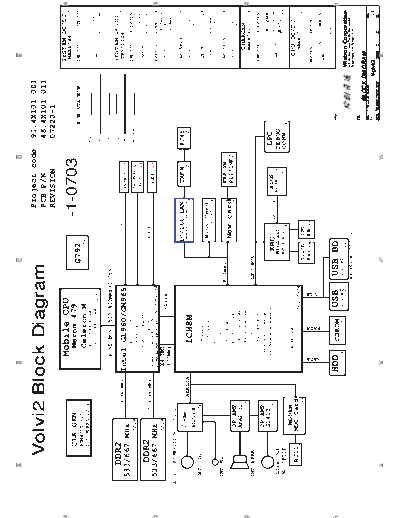
                Volvi2 Block Diagram                                                                                                           Project code: 91.4X101.001
                                                                                                                                               PCB P/N     : 48.4X101.011
                                                                                                                                               REVISION    : 07220-1

                                                                                                                                           -1-0703
4                                                            Mobile CPU                                                                                                                                                           SYSTEM DC/DC                                 4
                                                                                                                                                                                                                                    MAX8744                               31
                   CLK GEN.                                        Merom 479                                    G792                                                                      PCB STACKUP                             INPUTS                   OUTPUTS
                   RTM875T-605
                  (ICS 9LPRS502) 3
                                                                   Celeron M                                               20
                                                                  2.0G : 71.MEROM.A0U                                                                                          TOP
                                                                                                                                                                                                                                                        5V_S5(6A)
                                                                  2.33G : 71.MEROM.B0U                                                                                                                                            DCBATOUT
                                                                                                 4, 5                                                                          VCC                                                                      3D3V_S5(6A)


                                                             HOST BUS                  533/[email protected]                                                                         S

           DDR2                                                                                                                                                                 S                                                 SYSTEM DC/DC
                                533/667MHz                                                                                      SVIDEO/COMP                                                                                         TPS51124                              32
      533/667 MHz                                  Intel GL960/GM965                                                                                     TVOUT 15              GND
                                                                     AGTL+ CPU I/F                                                                                                                                                INPUTS                OUTPUTS
                        12,13                                                                                                   LVDS                     14" WXGA              BOTTOM
                                                                     DDR Memory I/F
                                                                                                                                                          LCD   14                                                                DCBATOUT
                                                                                                                                                                                                                                                      1D05V_S0(8A)
                                                              INTEGRATED GRAHPICS
               DDR2             533/667MHz                    LVDS, CRT I/F
                                                   GL960:71.GL960.A0U, QN79
                                                                                                                                RGB CRT
                                                                                                                                                                                                                                                      1D8V_S3(12A)

                                                                                                                                                           CRT       15
3     533/667 MHz                                  GM965:KI.96501.005, SLA5T               6,7,8,9,10,11                                                                                                                          TPS51100(G2997) 33                           3
                        12,13                                                                                                                                                                                                                           DDR_VREF_S0
                                                    X4 DMI                                                                                                                                                                        1D8V_S3
                                                                                           C-Link0                                                                                                                                                      (1.5A)
                                                    400MHz                                                                                                                                                                                              DDR_VREF_S3
    Audio BD REVISION:07551-1
                                                                                                                             10/100 LAN                    TXFM               RJ45                                                  APL5913                               33
                         Codec            AZALIA                                                                                Marvell 88E8039                      22              22
                         ALC268                                      ICH8M                                                                         22                                                                             1D8V_S3               1D25V_S0
                                                                                                                                                                                                                                                        (1.5A)

       MIC In                   24                                   6 PCIe ports                                                                                                                                                   G909                                  28
                                                                     PCI/PCI BRIDGE                                             Mini Card
                                                                                                                                         abgn/bg   23                                                                             5V_AUX_S5             3D3V_AUX_S5
      25                                                             ACPI 1.1                                                                                                                                                                           (100mA)

      INT.MIC                                                        3 SATA
                                                                                                           PCIex1                                          PWR SW                                                                   APL5915                               33
                                                                     1 PATA 66/100
                                                                     10 USB 2.0/1.1 ports
                                                                                                                                New card
                                                                                                                                       23                  P2231NFC
                                                                                                                                                                  23                                                              1D8V_S3               1D5V_S0
                         OP AMP                                                                                                                                                                                                                         (1.5A)
      25                                                          ETHERNET (10/100/1000MbE)
                         APA2031
2                                 25                                 High Definition Audio                                                                                                                                                   CHARGER                           2
                                                                                                                                                                                                                                             MAX8731                      34
      INT.SPKR                                                       LPC I/F                               LPC BUS
                                                                     Serial Peripheral I/F                                                                                                                                        INPUTS                OUTPUTS
                         OP AMP                               Matrix Storage Technology(DO)
                         G1412                                                                                                                                                                                                                          CHG_PWR
                                  25
                                                             Active Managemnet Technology(DO)
                                                                                                                         KBC              SPI I/F        BIOS                 LPC                                                                       18V       4.0A
       Line Out                                                                                                         Winbond                         W25X80-VSS                                                                DCBATOUT
                                                                                                                                                                              DEBUG                                                                     UP+5V
                                                                                                                        WPC8763L                               27                                                                                       5V  100mA
      (No-SPDIF)                                                                                                                    26                                        CONN. 36
                          MODEM                               71.ICH8M.A0U, QN23                                                                                                                                                       CPU DC/DC
               RJ11
                  22
                        MDC Card                                                             16,17,18,19                                                                                                                                     MAX8770
                                     21                                                                             Touch        INT.                                                                                                                                     30
                                                                                                   USB


                                                                                                                    Pad 27       KB 27
                                                      SATA


                                                                               PATA


                                                                                                                                                                                                                               INPUTS              OUTPUTS

                                                                                                                                                                                                                               DCBATOUT
                                                                                                                                                                                                                                        VCC_CORE_S0
                                                                                                                                                                                                                                                      0~1.3V
                                                                                                                                                                                                                                                       47A
1                                                  HDD                 CDROM                  USB           USB BD                                                                         RTM
                                                                                                                                                                                                                                                                               1
                                                             21                       21      1 PORT        2 PORT
                                                                                                   21                21                                                                                                       Wistron Corporation
                                                                                                                                                                                                                              21F, 88, Sec.1, Hsin Tai Wu Rd., Hsichih,
                                                                                                           REVISION:07570-1                                                                                                   Taipei Hsien 221, Taiwan, R.O.C.

                                                                                                                                                                                           Title

                                                                                                                                                                                                        BLOCK DIAGRAM
                                                                                                                                                                                           Size     Document Number                                                  Rev
                                                                                                                                                                                           A3
                                                                                                                                                                                                                           Volvi2                                         -1
                                                                                                                                                                                           Date: Thursday, July 05, 2007             Sheet     1         of          36
                            A                                               B                                           C                                                 D                                                            E
    ICH8M Functional Strap Definitions
                            ICH8-M EDS 21762                                 2.0V1      page 16
                                                                                                  ICH8M Integrated Pull-up                                               Crestline Strapping Signals and
     Signal         Usage/When Sampled                            Comment                         and Pull-down Resistors                                                Configuration       Crestline EDS 20954
                                                                                                                                                                                                        page 7
                                                                                                                                                                                                                                                                  1.0
                                                                                                                                  ICH8-M EDS 21762     2.0V1
    HDA_SDOUT    XOR Chain Entrance/       Allows entrance to XOR Chain testing when TP3                                                                          Pin Name      Strap Description                      Configuration
                 PCIE Port Config1 bit1,   pulled low.When TP3 not pulled low at rising edge
                 Rising Edge of PWROK      of PWROK,sets bit1 of RPC.PC(Config Registers:           SIGNAL                  Resistor Type/Value                   CFG[2:0]     FSB Frequency Select           001 = FSB533
                                           offset 224h)                                           HDA_BIT_CLK                 PULL-DOWN 20K                                                                   011 = FSB667
                                                                                                                                                                                                              010 = FSB800
                                                                                                  HDA_RST#                    NONE                                                                            others = Reserved
4   HDA_SYNC     PCIE config1 bit0,        This signal has a weak internal pull-down.
                                           Sets bit0 of RPC.PC(Config Registers:Offset 224h)                                                                      CFG[4:3]     Reserved
                                                                                                                                                                                                                                                                               4
                 Rising Edge of PWROK.                                                            HDA_SDIN[3:0]               PULL-DOWN 20K
    GNT2#        PCIE config2 bit0,        This signal has a weak internal pull-up.               HDA_SDOUT                   PULL-DOWN 20K                       CFG5         DMI x2 Select                  0 = DMI x2
                 Rising Edge of PWROK.     Sets bit2 of RPC.PC2(Config Registers:Offset 0224h)                                                                                                                1 = DMI x4      (Default)
                                                                                                  HDA_SYNC                    PULL-DOWN 20K                       CFG[8:6]     Reserved
    GPIO20       Reserved                  This signal should not be pulled high.
                                                                                                  GNT[3:0]                    PULL-UP 20K                                                                     0 = Normal mode
    GNT1#/       ESI Strap (Server Only)   ESI compatible mode is for server platforms only.                                                                                   Low Power PCI Express          1 = Low Power mode           (Default)
    GPIO51       Rising Edge of PWROK      This signal should not be pulled low for desttop       GPIO[20]                    PULL-DOWN 20K ?
                                           and mobile.                                                                                                                                                        0 = Reverse Lanes,15->0,14->1 ect..
                                                                                                  LDA[3:0]#/FHW[3:0]#         PULL-UP 20K                         CFG9         PCI Express Graphics           1= Normal operation(Default):Lane
                                                                                                                                                                               Lane Reversal                     Numbered in order
                 Top-Block                 Sampled low:Top-Block Swap mode(inverts A16 for        LAN_RXD[2:0]                PULL-UP 10K
    GNT3#        Swap Override.            all cycles targeting FWH BIOS space).
                 Rising Edge of PWROK.     Note: Software will not be able to clear the           LDRQ[0]                     PULL-UP 20K                         CFG[11:10]   Reserved
                                           Top-Swap bit until the system is rebooted                                                                                           XOR/ALL Z test                 00   =   Reserved
                                           without GNT3# being pulled down.                       LDRQ[1]/GPIO23              PULL-UP 20K
                                                                                                                                                                  CFG[13:12]   straps                         01   =   XOR mode enabled
                                                                                                  PME#                        PULL-UP 20K                                                                     10   =   All Z mode enabled
    GNT0#/       Boot BIOS Destination     Controllable via Boot BIOS Destination bit                                                                                                                         11   =   Normal Operation (Default)
    SPI_CS1#     Selection.                (Config Registers:Offset 3410h:bit 11:10).             PWRBTN#                     PULL-UP 20K
                 Rising Edge of PWROK.     GNT0# is MSB, 01-SPI, 10-PCI, 11-LPC.                                                                                  CFG[15:14]   Reserved                          Reserved
                                                                                                  SATALED#                    PULL-UP 15K
                 Integrated VccSus1_05,    Enables integrated VccSus1_05, VccSus1_5 and                                                                           CFG16        FSB Dynamic ODT                0 = Dynamic ODT Disabled
    INTVRMEN     VccSus1_5 and VccCL1_5    VccCL1_5 VRM's when sampled high                       SPI_CS1#                    PULL-UP 20K                                                                     1 = Dynamic ODT Enabled (Default)
                 VRM Enable/Disable.
                 Always sampled.                                                                  SPI_CLK                     PULL-UP 20K
                                                                                                                                                                  CFG[18:17]   Reserved
3                Integrated VccLAN1_05     Enables integrated VccLAN1_05 and VccCL1_05 VRM's
                                                                                                  SPI_MOSI                    PULL-UP 20K
                                                                                                                                                                                                              0 = Normal operation (Default):lane                              3
    LAN100_SLP   and VccCL1_05 VRM         when sampled high                                      SPI_MISO                    PULL-UP 20K                         CFG19        DMI Lane Reversal                  Numbered in order
                 Enable/Disable.
                 Always sampled.                                                                  TACH_[3:0]                  PULL-UP 20K ?                                                                   1 =Reverse Lane,4->0,3->1 ect...

                                                                                                  SPKR                        PULL-DOWN 20K                                                                   0 = Only SDVO or PCIE x1 is
                 PCI Express Lane          Signal has weak internal pull-up. Sets bit 27                                                                          CFG20         SDVO/PCIE                         operational (Default)
    SATALED#     Reversal. Rising Edge     of MPC.LR(Device 28:Function 0:Offset D8)              TP[3]                       PULL-UP 20K                                       Concurrent                    1 =SDVO and PCIE x1 are operating
                 of PWROK.                                                                                                                                                                                       simultaneously via the PEG port
                                                                                                  USB[9:0][P,N]               PULL-DOWN 15K
    SPKR         No Reboot.                If sampled high, the system is strapped to the                                                                         SDVOCRTL      SDVO Present                  0 = No SDVO Card present (Default)
                 Rising Edge of PWROK.     "No Reboot" mode(ICH8 will disable the TCO Timer       CL_RST#                     PULL-UP 13K                         _DATA
                                           system reboot feature). The status is readable                                                                                                                     1= SDVO Card present
                                           via the NO REBOOT bit.
                                                                                                                                                                  NOTE: All strap signals are sampled with respect to the leading
    TP3          XOR Chain Entrance.       This signal should not be pull low unless using                                                                                 edge of the Crestline GMCH PWORK in signal.
                 Rising Edge of PWROK.     XOR Chain testing.

    GPIO33/      Flash Descriptor          This signal has a weak internal pull-up.
                                                                                                    History
    HDA_DOCK     Security Override Strap   Sampled low:the Flash Descriptor Security will be
    _EN#         Rising Edge of PWROK      overridden. If high,the security measures will be        2007/05/02
                                           in effect.This should only be used in manufacturing      1 Based on Tahoe to modify schematics.
                                           environments.                                            ===========================================================
                                                                                                    2007/05/14
                                                                                                    1.Page 34:Replace "D25" with "BAS16-1-GP".
                                                                                                    2.Page 27:Replace "R485" with "2K7R2j".
2                                                                                                   3.Page 27:DY:C379"                                                                                                                                                         2
                                                                                                    4.Page 27:Add "C682" D1u capacitor on "LID1.PIN1"
    ICH8M IDE Integrated Series                                                                     5.Page 27:Replace "R238" with "0R2".
                                                                                                    6.Page 25:Replace "INTMIC1" & "SPKR1" with main source follow connector list.
                                                                                                    7.Page 5:Add C115, C116, C141, C149, C169, C171 for Colay with TC25.
    Termination Resistors                                                                           8.Page 10:Replace "L20" with "68.00217.141".
                                                                                                    9.Page 10:Replace "L10" & "L23" with "68.00217.101"
                                                                                                    ===========================================================
    DD[15:0], DIOW#, DIOR#, DREQ,
                                              approximately 33 ohm
    DDACK#,    IORDY, DA[2:0], DCS1#,
    DCS3#, IDEIRQ

                                                  USB Table
    PCIE Routing                                           USB
    LANE1      LAN Marvell                          Pair     Device
    LANE2      MiniCard WLAN                         0      USB1
    LANE3      NewCard WLAN                          1      NC
                                                     2      USB2
                                                     3      NC
1                                                                                                                                                                                         RTM
                                                                                                                                                                                                                                                                               1
                                                     4      USB3
                                                     5      NC                                                                                                                                                                Wistron Corporation
                                                                                                                                                                                                                              21F, 88, Sec.1, Hsin Tai Wu Rd., Hsichih,
                                                     6      NC                                                                                                                                                                Taipei Hsien 221, Taiwan, R.O.C.

                                                     7      MINICARD                                                                                                                      Title

                                                     8      CCD                                                                                                                                        Reference
                                                                                                                                                                                          Size     Document Number                                                   Rev
                                                     9      NEW1                                                                                                                          A3
                                                                                                                                                                                                                          Volvi2                                          -1
                                                                                                                                                                                          Date: Thursday, July 05, 2007              Sheet     2         of          36
                                  A                                                                                           B                                                                                C                                                                   D                                                                                E

                                                                                                                                                                                                                                                                                                                                                                                3D3V_S0
                                                                                                                                                                                                          -1                    3D3V_S0                                                                                                            -1         R74
    3D3V_S0        -1                                                                                                                                                                                              R63                                                                                                                                        0R0603-PAD
          0R0603-PAD                                                                                                                                                                                               0R0603-PAD                                                                                                        3D3V_CLKGEN_S0           1        2
          1        2       3D3V_48MPWR_S0                                                                                              3D3V_CLKPLL_S0                                                              1        2


                                                                                                                                                                                                                                                       1


                                                                                                                                                                                                                                                                              1


                                                                                                                                                                                                                                                                                                     1


                                                                                                                                                                                                                                                                                                                                 1


                                                                                                                                                                                                                                                                                                                                                       1
          R244                                                                                                                                                                                                                                             C154                    C403                   C393                       C409                   C399


                                             SC4D7U6D3V3KX-GP
                              1


                                                           1


                                                                               1


                                                                                                        1


                                                                                                                                   1


                                                                                                                                                              1


                                                                                                                                                                                    1


                                                                                                                                                                                                           1
                                      C407                      C404               C400                     C124                        C398                      C397                   C396                                                     DY                                                                                                        SCD1U16V2ZY-2GP
                                      DY                                                                                                                                                                        C394                                       SC4D7U10V5ZY-3GP        SCD1U16V2ZY-2GP        SCD1U16V2ZY-2GP            SCD1U16V2ZY-2GP


                                                                                                                                                                                                                                                       2


                                                                                                                                                                                                                                                                              2


                                                                                                                                                                                                                                                                                                     2


                                                                                                                                                                                                                                                                                                                                 2


                                                                                                                                                                                                                                                                                                                                                       2
                                                                                   SCD1U16V2ZY-2GP          SC4D7U10V5ZY-3GP            SCD1U16V2ZY-2GP           SCD1U16V2ZY-2GP        SCD1U16V2ZY-2GP        SCD1U16V2ZY-2GP


                              2


                                                      2


                                                                               2


                                                                                                        2


                                                                                                                                   2


                                                                                                                                                              2


                                                                                                                                                                                    2


                                                                                                                                                                                                           2
                                                           SC1U16V3ZY-GP


4                                                                                                                                                                                                                                                                                                                                                                                                            4
                                                                     3D3V_S0
                                                                                                                                                                                                                                U12

                                                                                                                                                                                    3D3V_CLKGEN_S0                          2                                                       55
                                                                                                                                                                                                                                                                                                                              -1_0628
                                                                                                                                                                                                                                VDDPCI                                    SDATA                      SMBD_ICH 12,19
                       2


                                              2


                                                                       2


                                                                                          2
                                                                                                                                                                                    3D3V_48MPWR_S0                          9                                                       56
                                                                DY             DY              DY                                                                                                                          16
                                                                                                                                                                                                                                VDD48                                      SCLK                       SMBC_ICH 12,19
                            R243                           R240            R233               R229                                                                                                                              VDD
                                                                                                                                                                                                                           53   VDDREF
                            10KR2J-3-GP                    10KR2J-3-GP     10KR2J-3-GP        10KR2J-3-GP                                                                                                                                                                           13    DREFCLK_1                          1            2                               DREFCLK 7
                                                                                                                                                                                                                                                             DOTT_96/SRCCLKT0             DREFCLK#_1                      R384       0R0402-PAD
                                                                                                                                                                                                                           31                                                       14                                       1            2                               DREFCLK# 7
                       1


                                              1


                                                                       1


                                                                                          1
                                                                                                                                                                                                                                VDDSRC                       DOTC_96/SRCCLKC0                                             R385       0R0402-PAD
                                                                                                                                                                                                                           47   VDDCPU
       PCLKCLK2                                                                                                                                                                                                                                                                     17    CLK_PCIE_NEW_R                     1            2                             CLK_PCIE_NEW 23
       PCLKCLK3                                                                                                                                                                         3D3V_CLKPLL_S0                                                              SRCCLKT1/SE1          CLK_PCIE_NEW#_R                 R386       0R0402-PAD
                                                                                                                                                                                                                           12   VDD96I/O                            SRCCLKC1/SE2    18                                       1            2                             CLK_PCIE_NEW# 23
       PCLKCLK4                                                                                                                                                                                                            20                                                                                             R387       0R0402-PAD
       PCLKCLK5                                                                                                                                                                                                                 VDDPLL3I/O                                                CLK_PCIE_SATA_1
                                                                                                                                                                                                                           26   VDDSRCI/O                   SRCCLKT2/SATACLKT       21                                       1            2                             CLK_PCIE_SATA 16
                                                                                                                                                                                                                           37                                                       22    CLK_PCIE_SATA_1#                R388
                                                                                                                                                                                                                                                                                                                             1       0R0402-PAD
                                                                                                                                                                                                                                                                                                                                          2                             CLK_PCIE_SATA# 16
                                                                                                                                                                                                                                VDDSRCI/O                   SRCCLKC2/SATACLKC                                             R389       0R0402-PAD
                                                                                                                                                                                                                           41   VDDCPUI/O
                       2


                                              2


                                                                       2


                                                                                          2
                                                                                                                                                                                                                                                                                    24    CLK_MCH_3GPLL_1                    1            2
                            DY                                  RTM                                                                                                               TPAD30 TP27             PCLKCLK0          1
                                                                                                                                                                                                                                                                  SRCCLKT3/CR#_C
                                                                                                                                                                                                                                                                                    25    CLK_MCH_3GPLL_1#                R390
                                                                                                                                                                                                                                                                                                                             1       0R0402-PAD
                                                                                                                                                                                                                                                                                                                                          2
                                                                                                                                                                                                                                                                                                                                                                        CLK_MCH_3GPLL 7
                                                                                                                                                                                                                                                                                                                                                                        CLK_MCH_3GPLL# 7
                            R242                           R236            R230               R231                                                                                                                              PCICLK0/CR#_A                     SRCCLKC3/CR#_D                                          R391       0R0402-PAD
                            10KR2J-3-GP                    10KR2J-3-GP     10KR2J-3-GP        10KR2J-3-GP                                                                         TPAD30 TP26             PCLKCLK1          3                                                       27    CLK_PCIE_MINI_12                   1            2                             CLK_PCIE_MINI1 23
                                                                                                                                                                                                                                PCICLK1/CR#_B                          SRCCLKT4           CLK_PCIE_MINI_12#               R392       0R0402-PAD
                                                                                                                                                                                                                                                                                    28                                       1            2                             CLK_PCIE_MINI1# 23
                       1


                                              1


                                                                       1


                                                                                          1


                                                                                                                                                                                                          PCLKCLK2                                                     SRCCLKC4                                           R393       0R0402-PAD
                                                                                                                                                              -1_0627                                                       4   PCICLK2/LTE
                                                                                                                                                                                                                                                                                    30
                                                                                                                                                                                                                                                            PCI_STOP#/SRCCLKT5                   PM_STPPCI# 17
                                                                                                                                                                                                          PCLKCLK3          5                                                       29           PM_STPCPU# 17
                                                                                                                                                                                                                                PCICLK3                    CPU_STOP#/SRCCLKC5
                                                                                                                                        26        PCLK_KBC               R238 2           1 22R2J-2-GP    PCLKCLK4          6                                                       33    CLK_PCIE_ICH_1                     1            2                             CLK_PCIE_ICH 17
                                                                                                                                                                                                                                PCICLK4/SRC5_EN                        SRCCLKT6           CLK_PCIE_ICH_1#                 R394       0R0402-PAD
                                                                                              CL=20pF


◦ Jabse Service Manual Search 2024 ◦ Jabse PravopisonTap.bg ◦ Other service manual resources online : FixyaeServiceinfo