Service Manuals, User Guides, Schematic Diagrams or docs for : acer Acer Aspire 5910_Wistron_Huron_Rev_SD

<< Back | Home

Most service manuals and schematics are PDF files, so You will need Adobre Acrobat Reader to view : Acrobat Download Some of the files are DjVu format. Readers and resources available here : DjVu Resources
For the compressed files, most common are zip and rar. Please, extract files with Your favorite compression software ( WinZip, WinRAR ... ) before viewing. If a document has multiple parts, You should download all, before extracting.
Good luck. Repair on Your own risk. Make sure You know what You are doing.


Image preview - the first page of the document
Acer Aspire 5910_Wistron_Huron_Rev_SD


>> Download Acer Aspire 5910_Wistron_Huron_Rev_SD documenatation <<

Text preview - extract from the document
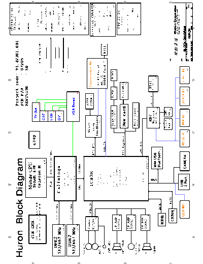
                A                                         B                                                       C                                                         D                                                           E
                                                                                                                                                                                                                                    SYSTEM DC/DC
                                                                                                                                                                                                                                      TPS51120

    Huron Block Diagram
                                                                                                                                                                                                                                                                            37
                                                                                                                                                  Project code: 91.4V301.001                                                        INPUTS                   OUTPUTS
                                                                                                                                                  PCB P/N     : 07205
                                                                                                                                                                                                                                                             5V_S5
                                                                                                                                                  REVISION    : SD
                                                      Mobile CPU
                                                                                                                                                                                                                                    DCBATOUT
                                                                                                                                                                                                                                                             3V_S5

4               CLK GEN.                               Yonah 478                                         G792                                                                                                                                                                    4
               IDTCV125PAG 71.00125.A0W                                                                                            TV Out
                                                                                                                                                                                                                                         SYSTEM DC/DC
               RTM865T-433 71.00865.B0W                Celeron M                                                20                                14
                                                                                                                                                                                              PCB STACKUP                                   TPS51124 38
                                3                             62.10079.001           4, 5                                         CRT
                                                                                                                                        14                                           TOP                                            INPUTS                OUTPUTS

                                                         FSB             400/533/667MHz                                           LCD                                                VCC
                                                                                                                                                                                                                                    DCBATOUT
                                                                                                                                                                                                                                                             1D8V_S3


         DDR2                                                                                                                           13                                                                                                                   1D05V_S0
                                                                                                                                                                                      S
                               533/667MHz
    533/667 MHz                                      Calistoga
                                                       AGTL+ CPU I/F
                                                                                                                                  DVI
                                                                                                                                        42
                                                                                                                                                                                      S
                                                                                                                                                                                                                                               TPS51100                     40
                     13,14                                                                                                                                                           GND                                            1D8V_S3                  DDR_VREF
                                                         DDR Memory I/F

         DDR2                  533/667MHz
                                                     INTEGRATED GRAHPICS
                                                         LVDS, CRT I/F
                                                                                                                                                                                     BOTTOM
                                                                                                                                                                                                                                               APL5308                      40
    533/667 MHz                                          71.CALIS.00U             6,7,8,9,10                                        VGA Borad                                                                                         3D3V_S0                   2D5V_S0

                     13,14                                                                                                                                  26
3                                                     DMI                100MHz                                                                                                                                                                APL5912                      39
                                                                                                                                                                                                                                                                                 3
    Line In                                                                                                                                                                                                                           1D8V_S3             1D5V_S0

                      Codec                                                                                       OZ129                           1394
                                      AZALIA
                      ALC268                             ICH7M                                 PCI BUS             1394
                                                                                                                                                  CONN   25            Cardreader BD                                           Intersil CHARGER
                                                                                                                                                                       PCB P/N:07517                                                        MAX8731                         41
                               28                        4 PCIe ports                                           CardReader                                             MS/MS Pro/xD/
    MIC In                                                                                                                   24                                                                                                  INPUTS                   OUTPUTS
                                                         PCI/PCI BRIDGE                                                                                                MMC/SD 5 in 1
    29                                                   ACPI 2.0                                   AZALIA                                                             MODEM Card             25         RJ11                                             BT+
                                                         2 SATA                                                                                                                                                                                           18V       4.0A
     INT.MIC                                             1 PATA 66/100
                                                                                                                                                                                                                                 DCBATOUT
                                                                                                                                                                                                                                                          UP+5V
                                                         8 USB 2.0/1.1 ports                                               Giga LAN 22                  TXFM                    RJ45                                                                      5V        100mA
                                                                                                                           BCM5787MKMLG
    29                OP AMP                          ETHERNET (10/100/1000MbE)
                                                                                                                                                                  23                 23
                      G1431Q 29                          High Definition Audio                                                                                                                                                           CPU DC/DC
                                                                                                                                                                                                                                               ISL6262
    INT.SPKR                                             LPC I/F                               PCI Express                 New card                     P2231NFC1                                                                                                   35
2                                                        Serial Peripheral I/F                                                     27                                  28                                                                                                        2
                      OP AMP                                                                                                                                                                                                     INPUTS              OUTPUTS
                      G1412                                                                                                                                                                                                                          VCC_CORE
                                                                                                                                                                                                                                 DCBATOUT
    Line Out
                                29                                                                                         Mini Card                                                                                                                    0~1.3V
                                                                                                                           Kedron a/b/g/n         27                                                                                                     48A
    (SPDIF)                                                                                     LPC BUS
                      OP AMP                               71.ICH7M.00U
    29                G1442                                                      15,16,17,18
                                29
                                                                                                                              KBC                 SPI I/F             BIOS
                                                                USB


                                                                                                                             Winbond                              W25X80-VSS
    SUBWF                                                                         MINI USB                                   WPC8768L                                           32
                                                                                                                                             30
                                         SATA                                     BlueTooth
                             HDD20
                                                                                                    22

                                                                                                                          Touch     INT.
                                              PATA                                                                        Pad 31    KB 31                                                      Volvi
1                                                                                                                                                                                                                                                                                1
                              CDROM
                                       20                                                                                                                                                                                       Wistron Corporation
                                                                                                                                                                                                                                21F, 88, Sec.1, Hsin Tai Wu Rd., Hsichih,
                                                                                                                                                                                                                                Taipei Hsien 221, Taiwan, R.O.C.


                                    USB BD               USB                                             MEDIA BD           PWM BD                 LAUNCH BD                e-Key BD           Title

                                    PCB : 07521          2 Port21                CAMERA                  56.41004.031       PCB : 07520            PCB : 07519              PCB : 07518                     BLOCK DIAGRAM
                                                                                                                                                                                               Size    Document Number                                                 Rev
                                              21                                               13                    31                 31                       31                   31       A3
                                                                                                                                                                                                                              HURON                                         SD
                                                                                                                                                                                               Date: Monday, March 12, 2007            Sheet     1         of          44
                            A                                                B                                                C                                              D                                                           E
    ICH7M Integrated Pull-up                                                                   RTM865T-433 100Mhz/LCDCLK Spread                                     Calistoga Strapping Signals and
    and Pull-down Resistors                             ICH7-M EDS 17837         1.5V1
                                                                                               and Frequency Selection Table                                        Configuration       EDS 17050 0.71
                                                                                                                                                                                                       page 7
                                                                                               SS3      SS2    SS1     SS0
                                                                                               Byte9    bit6   bit5    bit4       Spread Amount%           page 3    Pin Name      Strap Description                     Configuration
    EE_DIN, EE_DOUT, GNT[3:0], GPIO[25],                                                       bit 7                                                                 CFG[2:0]     FSB Frequency Select
    GNT[4]#/GPIO48, GNT[5]#/GPO17, PME#,                                                        0       0      0       0           0.8% Down                                                                     001 = FSB533
                                              ICH7 internal 20K pull-ups                                                                                                                                         011 = FSB667
    LAD[3:0]#/FHW[3:0]#, LAN_RXD[2:0]                                                           0       0      0       1           1.0% Down                                                                     others = Reserved

4   LDRQ[0], LDRQ[1]/GPIO[41],                                                                  0       0      1       0           1.25% Down                        CFG[4:3]     Reserved                                                                                         4
    PWRBTN#, TP[3]                                                                              0       0      1       1           1.50% Down                        CFG5         DMI x2 Select                  0 = DMI x2
                                                                                                                                                                                                                 1 = DMI x4     (Default)
                                                                                                0       1      0       0           1.75% Down                        CFG6         Reserved
    DD[7], DDREQ                              ICH7 internal 11.5K pull-downs
                                                                                                0       1      0       1           2.0% Down                         CFG7                                        0 = Reserved
                                                                                                                                                                                  CPU Strap                      1 =Mobile CPU(Default)
    ACZ_BIT_CLK, ACZ_RST#, ACZ_SDIN[2:0],     ICH7 internal 20K pull-downs                      0       1      1       0           2.5% Down
                                                                                                                                                                                  Reserved
    ACZ_SDOUT, ACZ_SYNC, DPRSLPVR/GPIO16,                                                       0       1      1       1           3.0% Down                         CFG8
    EE_CS,SPI_ARB, SPI_CLK, SPKR,                                                               1       0      0       0           +-0.3% Center                                                                 0 = Reverse Lanes,15->0,14->1 ect..
                                                                                                                                                                     CFG9         PCI Express Graphics           1= Normal operation(Default):Lane
                                                                                                1       0      0       1           +-0.4% Center                                  Lane Reversal                       Numbered in order
    USB[7:0][P,N]                             ICH7 internal 15K pull-downs
                                                                                                1       0      1       0           +-0.5% Center
                                                                                                                                                                     CFG[11:10]    Reserved
    SATALED#                                  ICH7 internal 15K pull-up                         1       0      1       1           +-0.6% Center
                                                                                                                                                                                  XOR/ALL Z test                 00 = Reserved
                                                                                                1       1      0       0           +-0.8% Center                     CFG[13:12]   straps                         01 = XOR mode enabled
    LAN_CLK                                   ICH7 internal 100K pull-down                                                                                                                                       10 = All Z mode enabled
                                                                                                1       1      0       1           +-1.0% Center                                                                 11 = Normal Operation
                                                                                                                                                                                                                 (Default)
                                                                                                1       1      1       0           +-1.25% Center
    ICH7M IDE Integrated Series                                                                 1       1      1       1           +-1.5% Center
                                                                                                                                                                     CFG[15:14]
                                                                                                                                                                     CFG16
                                                                                                                                                                                  Reserved
                                                                                                                                                                                  FSB Dynamic ODT
                                                                                                                                                                                                                    Reserved
                                                                                                                                                                                                                 0 = Dynamic ODT Disabled

3   Termination Resistors                                                                                                                                                         Global R-comp Disable
                                                                                                                                                                                                                 1 = Dynamic ODT Enabled (Default)
                                                                                                                                                                                                                 0 = All R-comp Disable                                            3
                                                                                                                                                                                                                 1 = Normal Operation (Default)
    DD[15:0], DIOW#, DIOR#, DREQ,
                                              approximately 33 ohm
                                                                                               PCI Routing                               page 16
                                                                                                                                                                     CFG17
                                                                                                                                                                     CFG18
                                                                                                                                                                                  (All R-comps)
                                                                                                                                                                                  VCC Select                     0 = 1.05V (Default)
    DDACK#,    IORDY, DA[2:0], DCS1#,                                                                                                                                                                            1 = 1.5V
    DCS3#, IDEIRQ
                                                                                                                    IDSEL     INT -> PIRQ           REQ/GNT          CFG19        DMI Lane Reversal              0 = Normal operation (Default):lane
                                                                                                                                                                                                                     Numbered in order
                                                                                                OZ129TZ              AD22      AG
                                                                                                                                                    REQ0# ->REQ0#
                                                                                                                                                                                                                 1 =Reverse Lane,4->0,3->1 ect...
                                                                                                                                                                                                                 0 = Only SDVO or PCIE x1 is
    ICH7M Functional Strap Definitions                                             page 16
                                                                                                                                                                     CFG20         SDVO/PCIE
                                                                                                                                                                                   Concurrent
                                                                                                                                                                                                                     operational (Default)
                                                                                                                                                                                                                 1 =SDVO and PCIE x1 are operating
                                                                                                                                                                                                                    simultaneously via the PEG port
     Signal          Usage/When Sampled                         Comment
                                                                                                                                                                     SDVOCRTL      SDVO Present                  0 = No SDVO Card present
    ACZ_SDOUT    XOR Chain Entrance/       Allows entrance to XOR Chain testing when TP3                                                                             _DATA                                           (Default)
                 PCIE Port Config bit1,    pulled low.When TP3 not pulled low at rising edge                                                                                                                     1= SDVO Card present
                 Rising Edge of PWROK      of PWROK,sets bit1 of RPC.PC(Config Registers:
                                                                                                                                                                    NOTE: All strap signals are sampled with respect to the leading
                                           offset 224h)
                                                                                                        PCIE Routing                                                      edge of the Calistoga GMCH PWORK in signal.
    ACZ_SYNC     PCIE bit0,                Sets bit0 of RPC.PC(Config Registers:Offset 224h)                LANE1     LAN BCM5787M
                 Rising Edge of PWROK.
                                                                                                            LANE2     MiniCard WLAN
    EE_CS        Reserved                  This signal should not be pull high.
                                                                                                            LANE3     NewCard WLAN
    EE_DOUT      Reserved                  This signal should not be pull low.
2   GNT2#        Reserved                  This signal should not be pull low.                                                                                                                                                                                                     2
                 Top-Block                 Sampled low:Top-Block Swap mode(inverts A16 for
    GNT3#        Swap Override.
                 Rising Edge of PWROK.
                                           all cycles targeting FWH BIOS space).
                                           Note: Software will not be able to clear the                USB Table
                                           Top-Swap bit until the system is rebooted
                                           without GNT3# being pulled down.                            USB ports definition
                                                                                                       Pair    Device
    GNT5#/       Boot BIOS Destination     Controllable via Boot BIOS Destination bit
    GPIO17#,     Selection.                (Config Registers:Offset 3410h:bit 11:10).                   0      USB1
    GNT4#/       Rising Edge of PWROK.     GNT5# is MSB, 01-SPI, 10-PCI, 11-LPC.
    GPIO48                                                                                              1      USB3
                                                                                                        2      USB2
    DPRSLPVR     Reserved                  This signal should not be pull high.
                                                                                                        3      USB4
    GPIO25       Reserved.
                 Rising Edge of RSMRST#.   This signal should not be pull low.                          4      MINICARD
    INTVRMEN     Integrated VccSus1_05     Enables integrated VccSus1_05 VRM when                       5      BlueTooth
                 VRM Enable/Disable.       sampled high
                 Always sampled.                                                                        6      CCD
    LINKALERT#   Reserved                  Requires an external pull-up resistor.                       7      NewCard
    REQ[4:1]#    XOR Chain Selection.
                 Rising Edge of PWROK.     TBD, Chapter 8.                                                                                                                                     
1                                                                                                                                                                                                                                                                                  1
    SATALED#     Reserved                  This signal should not be pull low.
    SPKR         No Reboot.                If sampled high, the system is strapped to the                                                                                                                                        Wistron Corporation
                 Rising Edge of PWROK.     "No Reboot" mode(ICH7 will disable the TCO Timer                                                                                                                                      21F, 88, Sec.1, Hsin Tai Wu Rd., Hsichih,
                                                                                                                                                                                                                                 Taipei Hsien 221, Taiwan, R.O.C.
                                           system reboot feature). The status is readable
                                           via the NO REBOOT bit.                                                                                                                              Title

    TP3          XOR Chain Entrance.       This signal should not be pull low unless using
                                                                                                                                                                                                                              Reference
                 Rising Edge of PWROK.     XOR Chain testing.                                                                                                                                  Size    Document Number                                                  Rev
                                                                                                                                                                                                                              HURON                                           SD
                                                                                                                                                                                               Date: Monday, March 12, 2007             Sheet     2         of          44
                                A                                                                                                                      B                                                                                                             C                                                                                                                                                               D                                                                      E


                                                                                                                                                                                                                                                                                                                                                                                                                                                                            RN9
                                                                                                                                                                                                                                                                                                                                                                                                                                                                            SRN33J-5-GP-U
                                                                                                                                                                                                                                                                                                                                                                                                                                                      DREFSSCLK_1       2            3            DREFSSCLK 7
                                                                                                                                                                                                                                                                                                                                                                                                                                                      DREFSSCLK#_1      1     UMA 4               DREFSSCLK# 7
                                                                                                                            R244      3D3V_S0                                                                               R75       3D3V_S0                                                                                                                   R252      3D3V_S0
                                                                                                                            0R0603-PAD                                                                                      0R0603-PAD                                                                                                                          0R0603-PAD                                                                                                  RN10
                                                         3D3V_CLKPLL_S0                                                     1        2                                 3D3V_48MPWR_S0                                       1        2                                                                      3D3V_CLKGEN_S0                                      1        2                                                                                                  SRN33J-5-GP-U
                                                                                                                                                                                                                                                                                                                                                                                                                                                     CLK_MCH_3GPLL_1 2               3            CLK_MCH_3GPLL 7


                                                    1


                                                                                    1


                                                                                                             1


                                                                                                                                                                   1


                                                                                                                                                                                                    1


                                                                                                                                                                                                                                                         1


                                                                                                                                                                                                                                                                                1


                                                                                                                                                                                                                                                                                                        1


                                                                                                                                                                                                                                                                                                                                1


                                                                                                                                                                                                                                                                                                                                                           1


                                                                                                                                                                                                                                                                                                                                                                                                         1
                                                         C383                           C382                     C66                                                     C106                           C107                                                 C92                    C71                     C63                     C100                        C96                                          C397                                    CLK_MCH_3GPLL_1# 1              4            CLK_MCH_3GPLL# 7


                                                         SC4D7U6D3V3KX-GP


                                                                                        SC1U16V3ZY-GP


                                                                                                                 SCD1U16V2ZY-2GP


                                                                                                                                                                         SC4D7U6D3V3KX-GP


                                                                                                                                                                                                        SC1U16V3ZY-GP
                                                                                                                                                                                                        SC1U16V3ZY-GP


                                                                                                                                                                                                                                                             SC4D7U6D3V3KX-GP


                                                                                                                                                                                                                                                                                    SCD1U16V2ZY-2GP


                                                                                                                                                                                                                                                                                                            SCD1U16V2ZY-2GP


                                                                                                                                                                                                                                                                                                                                    SCD1U16V2ZY-2GP


                                                                                                                                                                                                                                                                                                                                                                SCD1U16V2ZY-2GP
                                                                                                                                                                                                                                                                                                                                                                SCD1U16V2ZY-2GP


                                                                                                                                                                                                                                                                                                                                                                                                                 SCD1U16V2ZY-2GP
                                                                                                                                                                                                                                                                                                                                                                                                                 SCD1U16V2ZY-2GP
                                                    DY                                                                                                             DY


                                                    2


                                                                                    2


                                                                                                             2


                                                                                                                                                                   2


                                                                                                                                                                                                    2


                                                                                                                                                                                                                                                         2


                                                                                                                                                                                                                                                                                2


                                                                                                                                                                                                                                                                                                        2


                                                                                                                                                                                                                                                                                                                                2


                                                                                                                                                                                                                                                                                                                                                           2


                                                                                                                                                                                                                                                                                                                                                                                                         2
4                                                                                                                                                                                                                                                                                                                                                                                                                                                                           RN11                                                                    4
                                                                                                                                                                                                                                                                                                                                                                                                                                                                            SRN33J-5-GP-U
                                                                                                                                                                                                                                                                                                                                                                                                                                                      CLK_PCIE_ICH_1 2               3            CLK_PCIE_ICH 16
                                                                                                                                                                                                                                                                                                                                                                                                                                                      CLK_PCIE_ICH_1# 1              4            CLK_PCIE_ICH# 16

                                                                                                                                                                                                                                                                                                                                                                                                                                                                            RN12
                                                                                                                                                                                                                                                                                                                                                                                                                                                                            SRN33J-5-GP-U
                                                                                                                                                                                                                                                                                                                                                                                                                                                      CLK_PCIE_NEW_R 2               3            CLK_PCIE_NEW 27
                                                                                                                                                                                                                                                                                                                                                                                                                                                      CLK_PCIE_NEW#_R 1       NEW 4               CLK_PCIE_NEW# 27

                                                                                                                                                                                                                                                                                                                                                                                                                                                                            RN13
                                                                                                                                                                                                                                                                                                                                                                                                                                                                            SRN33J-5-GP-U
                                                                                                                                                                                                                                                                                                                                                                                                                                                      CLK_PCIE_SATA_1 2              3            CLK_PCIE_SATA 15
                                                                                                                                                                                                                                                                                                                                                                                                                                                      CLK_PCIE_SATA_1#1              4            CLK_PCIE_SATA# 15

                                                                                                                                                                                                                                                                                                                                                                                                                                                                            RN6
                                                                                                                                                                                                                                                                                                                                                                                                                                                                            SRN33J-5-GP-U
                                       3D3V_S0                                                                                                                                                                                                                                                                                                                                                                                                        CLK_PCIE_LAN#_R 2              3            CLK_PCIE_LAN# 22
                                                    H/L: 100/96MHz                                                                                                                                                                                                                                                                                                                                                                                    CLK_PCIE_LAN_R 1               4            CLK_PCIE_LAN 22
                                                                                                                                                                                                                                               U11
                                          1


                                              R72                                                                                  30         PCLK_KBC           1 R49                      2 33R2J-2-GP                    PCLKKBC       56                                                                                                          17       DREFSSCLK_1                                                                                                  RN5
                                              10KR2J-3-GP                                                                                                                                                                                      PCI_2/REQ_SEL                                              SRC_0/DOT96SS                                        DREFSSCLK#_1                                                                                                 SRN33J-5-GP-U
                                                                                                                                                                                                                                           3   PCI_3                                                    SRC_0#/DOT96SS#                               18
                                                                                                                                   24         PCLK_PCM           1 R64                      2 33R2J-2-GP                    PCLKPCM        4   PCI_4
                                                                                                                                                                                                                                                                                                                                                                                                                                                      CLK_PCIE_MINI_1# 2             3            CLK_PCIE_MINI1# 27
                                                                                                                                                                                                                                           5                                                                                                          19       CLK_MCH_3GPLL_1                                                                        CLK_PCIE_MINI_1 1              4            CLK_PCIE_MINI1 27
                                          2


                                                                                                                                                                                                                                               PCI_5                                                               SRC_1                                       CLK_MCH_3GPLL_1#
                                                                                                                                                                                                                                                                                                                  SRC_1#                              20
3                                             SS_SEL                                                                                                                                                                        SS_SEL        9                                                                                                           22       CLK_PCIE_ICH_1                                                                                                                                                                       3
                                                                                                                                                                                                                                               PCIF_1/DOT96SS_SEL#                                                 SRC_2
                                                                                                                                   16    CLK_ICHPCI              1 R65                      2 33R2J-2-GP                    PCLKICH       8    PCIF_0/ITP_EN                                                      SRC_2#                              23       CLK_PCIE_ICH_1#                                                                                          RN4
                                                                                                                                                                                                                                                                                                                                                      24       CLK_PCIE_NEW_R                                                                                           SRN33J-5-GP-U
                                                                                                                                                                                                                                                                                                                   SRC_3
                                          1


                                                                                                                                                                                            16 PM_STPPCI#                                 55                                                                                                          25       CLK_PCIE_NEW#_R                                                                        CLK_PCIE_PEG_1# 2          3                CLK_PCIE_PEG# 26
                                              R66                                                                                                                                                                                              PCI_STOP#                                                          SRC_3#                                       CLK_PCIE_SATA_1                                                                        CLK_PCIE_PEG_1 1


◦ Jabse Service Manual Search 2024 ◦ Jabse PravopisonTap.bg ◦ Other service manual resources online : FixyaeServiceinfo