Service Manuals, User Guides, Schematic Diagrams or docs for : acer Aspire 3650_travelmate 2450 S.G_AS3650_TM2450_ALL S.G_AS3650_TM2450_CH5
<< Back | HomeMost service manuals and schematics are PDF files, so You will need Adobre Acrobat Reader to view : Acrobat Download Some of the files are DjVu format. Readers and resources available here : DjVu Resources
For the compressed files, most common are zip and rar. Please, extract files with Your favorite compression software ( WinZip, WinRAR ... ) before viewing. If a document has multiple parts, You should download all, before extracting.
Good luck. Repair on Your own risk. Make sure You know what You are doing.
Image preview - the first page of the document
>> Download S.G_AS3650_TM2450_CH5 documenatation <<
Text preview - extract from the document
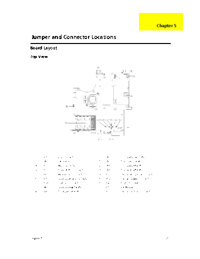
                                                                                          Chapter 5

Jumper and Connector Locations
Board Layout
Top View


   1        JP1    LCD Connector              10   SW7    Touchpad Down Button
   2        SW1    Lid Switch                 11   SW2    Touchpad Up Button
   3        JP3    MDC Connector              12   SW5    Touchpad Left Button
   4        JP2    Power Button Connector     13   SW3    Touchapd Left Button
   5        JP6    Media Board Connector      14   JP13   Internal Microphone Connector
   6        JP7    Touchpad Board Connector   15   JP12   Internal Speaker Connector
   7        JP43   SIM Card Connector         16   JP9    PCMCIA Socket
   8        SW4    Touchpad Right Button      17   IR1    FIR Module
   9        SW6    Touchpad Left Button       18   JP8    Internal Keyboard Connector


Chapter 5                                                                                     91
Bottom View


     NOTE: This is engineering sample. The image above may not be exactly the same as the real main board you
          get.


     1    JP19    FAN Connector                      17    JP40    Headphone/SPDIF Jack
     2    U42     VGA Chipset                        18    JP41    Line-In Jack
     3    JP18    CPU Socket                         19    JP42    Microphone-in Jack
     4    JP16    DVI Connector                      20    IR2     CIR Module
     5    JP15    CRT Connector                      21    SW8     Wireless LAN Switch
     6    JP14    TV-Out Connector                   22    SW9     Bluetooth and 3G Switch
     7    PCN1    DC-IN Jack                         23    U48     South Bridge Chipset
     8    JP17    Mini Card Connector                24    JP30    Mini Card Connector
     9    JP22    DDRII so-DIMM Socket               25    JP29    IEEE 1394 Connector
     10   JP21    DDRII so-DIMM Socket               26    JP27    5 IN1 Socket
     11   J3      Clear CMOS Jumper                  27    JP23    RJ45 Connector
     12   JP24    ODD Connector                      28    JP5     USB Connector
     13   PJP1    Battery Connector                  29    JP4     USB Connector
     14   JP32    HDD Connector (SATA)               30    JP28    MINIPCI Connector (TV-Tuner)
     15   JP33    HDD Connector (PATA)               31    JP25    FAN Connector
     16   JP36    Bluetooth Connector                32    U40     North Bridge Chipset


92                                                                                                  Chapter 5
Jumper Board Layout
Switch Board Top View


            Label              Description
    SW1                Arcade/TV tunver switch
    SW2                Volume Up switch
    SW3                Volume Down switch
    SW4                Play/Pause switch
    SW5                Stop switch
    SW6                Forward/Next switch
    SW7                Backward/Previous switch


Media Board Top View


            Label              Description
    SW1                Power Button
    SW2                E-mail Button
    SW3                Internet Button
    SW4                User Button
    SW5                E-Power Button


Chapter 5                                         93
Media Board Bottom View


           Label           Description
     JP3            USB Connector
     JP2            USB Connector
     JP6            RF INe Connector
     JP5            RF Cable Connector
     JP4            AV IN Connector
     JP7            Board to Main Board
                    Connector


LS-2923P Power Board Top View


           Label           Description
     JP1            SIM Card Connector


94                                        Chapter 5
Jumper Setting


            Label           Description
    J3              Clear CMOS Jumper
                    Note: J3 locates at bottom
                    side of the main board as
                    the red circle highlighted.


Chapter 5                                         95
96   Chapter 5
◦ Jabse Service Manual Search 2026 ◦ Jabse Pravopis ◦ onTap.bg ◦ Other service manual resources online : Fixya ◦ eServiceinfo