Service Manuals, User Guides, Schematic Diagrams or docs for : clarion DXZ-558MP clarion_dxz558rmp_905

<< Back | Home

Most service manuals and schematics are PDF files, so You will need Adobre Acrobat Reader to view : Acrobat Download Some of the files are DjVu format. Readers and resources available here : DjVu Resources
For the compressed files, most common are zip and rar. Please, extract files with Your favorite compression software ( WinZip, WinRAR ... ) before viewing. If a document has multiple parts, You should download all, before extracting.
Good luck. Repair on Your own risk. Make sure You know what You are doing.


Image preview - the first page of the document
clarion_dxz558rmp_905


>> Download clarion_dxz558rmp_905 documenatation <<

Text preview - extract from the document
                                  Xiamen Clarion Electrical Enterprise Co., Ltd
                                  8/F., Xiamen Mail Processing Centre, No.275 Rujiang Road, Xiamen, China                           Published by Service Dept.
                                  Tel:+86-592-2389080 Fax:+86-592-2389089                                                           298-6193-00 DEC.2004P
                                  Clarion Co., Ltd.
                                                                                                                                    Printed in P.R.C.
                                  50 Kamitoda , Toda-shi, Saitama 335-8511 Japan
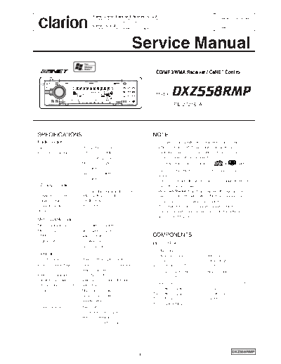


                                                                     Service Manual
                                                                                             CD/MP3/WMA Receiver / CeNET Control


                                                                                             Model

                                                                                                            (PE-2721E-A )


SPECIFICATIONS                                                                          NOTE
Radio section                                                                           *    We cannot supply PWB with component parts in principle.
Tuning system:             PLL synthesizer tuner                                             When a circuit on PWB has failure, please repair it by
Receiving frequencies:     FM 87.5 to 108MHz                                                 component parts base. Parts which are not mentioned in
                               (0.05MHz steps)                                               service manual are not supplied.
                           MW 531 to 1602kHz                                            *    Use only compact discs bearing the         or         mark.
                               (9kHz steps)
                                                                                             Some CDs recorded in CD-R/CD-RW mode may not be
                           LW 153 to 279kHz
                                                                                             usable.
                               (3kHz steps)
                                                                                        *    Specif ications and design are subject to change without notice
CD player section                                                                             for further improvement.
System:                    Compact disc digital audio system                            *                          , and the Windows      logo are trade-
Frequency response:        5Hz to 20kHz(+1/-1dB)                                             marks, or registerd trademarks of Microsoft Corporation
Signal to noise ratio:     100dB(1kHz)                                                       in the United States and/or other countries.
Dynamic range:             95dB(1kHz)                                                   *    This product includes technology owned by Microsoft
Distortion:                0.01%                                                             Corporation and cannot be used or distributed withouta
                                                                                             license from MSLGP.
MP3 / WMA mode
MP3 Sampling rate:         11.025kHz to 48kHz
MP3 Bit rate:              8k to 320kbps/VBR
WMA Bit rate:              48k to 192kbps                                               COMPONENTS
Logical Format:            ISO9660 level1, 2
                                                                                        PE-2721E-A
                           Romeo or Joliet
                                                                                        1.    Main unit                                                  1
General                                                                                 2.    Mounting bracket               300-7742-00                 1
Output power:               25Wx4 (DIN45324, +B=14.4V)                                  3.    DCP case                       335-6035-20                 1
Power supply voltage:       14.4V DC(10.8 to 15.6V allowable),                          4.    Escutcheon(OUT-ES)             370-6150-00                 1
                            negative ground
                                                                                        5. Remote control unit               RCB-172-300                 1
Power consumption:          Less than 15A
                                                                                        6. Battery(CR2025)                                               1
Speaker impedance:          4ohm(4ohm to 8ohm allowable)
                                                                                        7. Parts bag                                                     1
Auto antenna rated current: 500mA or less
                                                                                        7-1   Removal key                    331-2497-00                 2
Weight:                     Main unit    1.3kg
                                                                                        7-2   Rubber part                    345-3653-20                 1
                            Remote control unit
                                                                                        7-3   A-lead                         850-6681-50                 1
                            40g(including battery)
                                                                                        7-4   Screw(M5x10)                   716-0726-01                 1
Dimensions(mm):             Main unit
                            178(W)x50(H)x157(D)mm
                            Remote control unit
                            44(W)x110(H)x11(D)mm


                                                                                                                                              DXZ558RMP
                                                                          -1-
                                                                            9. Cautions in handling the optical pickup
To engineers in charge of repair or inspe-
                                                                               The laser diode of the optical pickup can be damaged by electr-
ction of our products.                                                         ostatic charge caused by your clothes and body. Make sure to
Before repair or inspection, make sure to follow the in-                       avoid electrostatic charges on your clothes or body, or discharge
structions so that customers and Engineers in charge                           static electricity before handling the optical pickup.
of repair or inspection can avoid suffering any risk or                     9-1. Laser diode
injury.                                                                          The laser diode terminals are shorted for transportation in ord-
1. Use specified parts.                                                          er to prevent electrostatic damage. After replacement, open
   The system uses parts with special safety features against fire               the shorted circuit.
   and voltage. Use only parts with equivalent characteristics when              When removing the pickup from the mechanism, short the ter-
   replacing them.                                                               minals by soldering them to prevent this damage.
  The use of unspecified parts shall be regarded as remodeling for          9-2. Actuator
  which we shall not be liable. The onus of product liability (PL) sh-           The actuator has a powerful magnetic circuit. If a magnetic
  all not be our responsibility in cases where an accident or failure            material is put close to it. Its characteristics will change.
   is as a result of unspecified parts being used.                               Ensure that not foreign substances enter through the ventilati-
2. Place the parts and wiring back in their original positions after re-         on slots in the cover.
   placement or re-wiring.                                                  9-3. Cleaning the lens
  For proper circuit construction, use of insulation tubes, bonding,             Dust on the optical lens affects performance.
  gaps to PWB, etc, is involved. The wiring connection and routing               To clean the lens, apply a small amount of isopropyl alcohol to
  to the PWB are specially planned using clamps to keep away                     lens paper and wipe the lens gently.
   from heated and high voltage parts. Ensure that they are placed
   back in their original positions after repair or inspection.
   If extended damage is caused due to negligence during repair,
   the legal responsibility shall be with the repairing company.
                                                                            CAUTION
                                                                            This appliance contains a laser system and is classified as a
3. Check for safety after repair.
                                                                            "CLASS 1 LASER PRODUCT". In case of any trouble with this
   Check that the screws, parts and wires are put back securely in
                                                                            player, please contact your nearest"authorized service station".
   their original position after repair. Ensure for safety reasons there
                                                                            To prevent direct exposure to the laser beam, do not try to open
   is no possibility of secondary problems around the repaired spots.
                                                                            the enclosure.
   If extended damage is caused due to negligence of repair, the
   legal responsibility shall be with the repairing company.
4. Caution in removal and making wiring connection to the parts for
   the automobile.
   Disconnect the battery terminal after turning the ignition key off.
   If wrong wiring connections are made with the battery connected,
   a short circuit and/or fire may occur.
   If extensive damage is caused due to negligence of repair, the
   legal responsibility shall be with the repairing company.
5. Cautions regarding chips.
   Do not reuse removed chips even when no abnormality is obser-
   ved in their appearance. Always replace them with new ones.
   (The chip parts include resistors, capacitors, diodes, transistors,
   etc). The negative pole of tantalum capacitors is highly suscepti-
   ble to heat, so use special care when replacing them and check
   the operation afterwards.
6. Cautions in handling flexible PWB
   Before working with a soldering iron, make sure that the iron tip
   temperature is around 270 C. Take care not to apply the iron tip
   repeatedly(more than three times) to the same patterns. Also ta-
   ke care not to apply the tip with force.                                                      Bottom view of main unit
7. Turn the unit OFF during disassembly and parts replacement.
   Recheck all work before you apply power to the unit.
8. Cautions in checking that the optical pickup lights up.
   The laser is focused on the disc reflection surface through the
   lens of the optical pickup. When checking that the laser optical
   diode lights up, keep your eyes more than 30cms away from the
   lens. Prolonged viewing of the laser within 30cms may damage
  your eyesight.


DXZ558RMP
                                                                           -2-
                                                                                  with insulation tape to prevent the risk of short-circuits.
NOTES OF ISO CONNECTOR
                                                                                  (Figure 2)
1. For VW and Audi vehicles, change the position of fuse                             Note: Before cutting the lead wire, disconnect the car battery
   installation as shown on the diagram.(Figure 1)                                         - (negative) cable.
  ISO CONNECTOR type

        For other vehicles
         (initial position)              For VW and Audi vehicles


                                                                    FUSE


                      Main unit side ISO connector
                                                                                               Figure 2
                              Figure 1


2. When the car stereo is installed in 1998 and later Volkswagen
   models, make sure to cut the car lead wire connected the A-5                   3. When the Main unit is also connected to an external amplifier,
   terminal. (A breakdown could occur if the lead wire is not cut.)                  connect REMOTE on the external amplifier to remote turn on
   After cutting the lead wire, insulate the front end of the lead wire              lead.


ERROR DISPLAY
If an error occurs, one of the following displays is displayed. Take the measures described below to eliminate the
problem.

   Mode          Error Display                                      Cause                                                Measure
                     ERROR 2             A DISC is caught inside the CD deck and is not ejected. This is a failure of CD deck's mechanism.

 CD/MP3/             ERROR 3             A DISC cannot be played due to scratches, etc.            Replace with a non-scratched, non-warped-disc.
  WMA                ERROR 6             A DISC is loaded upside-down inside the CD deck and       Eject the disc then reload it properly.
                                         does not play.

                     ERROR 2             A CD inside the CD changer is not loaded.                 This is a failure of CD changer's mechanism.

   CD                ERROR 3             A CD inside the CD changer cannot be played due to        Replace with a non-scratched, non-warped disc.
                                         scratches, etc.
 changer
                     ERROR 6             A CD inside the CD changer cannot be played beca-         Eject the disc then reload it properly.
                                         use it is loaded upside-down.

                     ERROR 2             A DISC inside the DVD changer cannot be played.            This is a failure of DVD mechanism.

                     ERROR 3             A DISC cannot be played due to scratches, etc.            Retry or replace with a non-scratched, non-warped
   DVD                                                                                             disc.
 changer
                     ERROR 6             A DISC inside the DVD changer cannot be played be-         Eject the disc then reload it properly.
                                         cause it is loaded upside-down.
                    ERROR P              Parental level error.                                      Set the correct Parental level.

                    ERROR R              Region code error.                                         Eject the disc and replace correct region code
                                                                                                    disc.


If an error display other than the ones described above appears, press the reset button.


Performing a system check                                                         ANTI-THEFT INDICATOR
1. Press the [ADJ] button to switch to the adjustment selection                   The red Anti-theft indicator is a function for preventing theft.
   display.                                                                       When the DCP is removed from the unit, this indicator blinks.
2. Press the [    ,   ] lever upward or downward to select the                    1. Press the [ADJ] button to switch to thead justment selection
   "SYS CHK ".                                                                    display.
3. Press and hold the [ ] button for 1 second or longer.                          2. Press the [   ,    ] lever upward or downward to select the
   "SYSTEM CHK" appears in the display, then the unit returns                        "BLINK LED".
   to the previous operation mode.                                                3. Turn the [ROTARY] knob to select "ON " or "OFF ".


                                                                                                                                       DXZ558RMP
                                                                            -3-
TROUBLESHOOTING

                   Problem                                  Cause                                         Measure

                                           Fuse is blown.                      Replace with a fuse of the same amperage.
             Power does not turn on.
             (No sound is produced.)
                                           Incorrect wiring.                   Read the attached "Installation/Wire connection Guide" once again
                                                                               and wire properly.

             No sound output when          Power antenna lead is shorted       1. Turn the unit off.
             operating the unit with       to ground or excessive current      2. Remove all wires attached to the power antenna lead. Check
             amplifiers or power           is required for remote-on the         each wire for a possible short to ground using an ohm meter.
             antenna attached.             amplifiers or power antenna.        3.Turn the unit back on.
                                                                               4. Reconnect each amplifier remote wire to the power antenna lead
                                                                                  one by one. If the amplifiers turn off before all wires are attached,
General


                                                                                  use an external relay to provide remote-on voltage
                                                                                  (excessive current required).

             Nothing happens when          The microprocessor has              Turn off the power, then press the                     Reset button
             buttons are pressed.          malfunctioned due to noise,         [OPEN] button and remove the DCP.
                                           etc.                                Press the reset button for about 2 seconds
             Display is not accurate.                                          with a thin rod.


                                           DCP or main unit connectors         Wipe the dirt off with a soft cloth moistened with cleaning alcohol.
                                           are dirty.


             No sound heard.               The speaker protection circuit is   Turn down sound volume. Function can also be restored by turning
                                           operating.                          the power off and on again.
                                                                               (Speaker volume is reduced automatically when the speaker prote-
                                                                               ction circuit operates).


             No sound heard.               MP3/WMA files are absent in         Write MP3/WMA files onto the disc properly.
                                           a disc.


                                           Files are not recognized as an      Use MP3/WMA files encoded properly.
                                           MP3/WMA file.

                                           File system is not correct.         Use ISO9660 level 1,2 or Joliet or Romeo file system.

             Sound skips or is noisy.      Disc is dirty.                      Clean the disc with a soft cloth.
CD/MP3/WMA


                                           Disc is heavily scratched or        Replace with a disc with no scratches.
                                           warped.

             Sound is cut or skipped.      MP3/WMA files are not               Use MP3/WMA files encoded properly.
             Noise is generated or noise   encoded properly.
             is mixed with sound.

             Sound is bad directly after   Water droplets may form on          Let dry for about 1 hour with the power on.
             power is turned on.           the internal lens when the car
                                           is parked in a humid place.

             Wrong filename                File system is not correct.         Use ISO9660 level 1, 2 or JOLIET or Romeo file system.

             Play list play is not         File name or extension is not       Use alphanumeric/ASCII characters for MP3/WMA file name.
             performed.                    correct.                            Use ".M3U" for the file extension of a play list.


DXZ558RMP
                                                                               -4-
ADJUSTMENT
FM section
Item                Procedure                                                                                                                 Measuring
                                                                                                                                              instrument
S-meter             1.Input the 98.1MHz/30dBu/400Hz(main90%+pilot10%)signal.                                                                  SG
                    2.Turn on the power and press the A-M button & PRESET No.6 button at the same
                       time for 1 second or longer.(TEST MODE)
                    3.Adjust the reading of LCD display to [24---- ](24+2/-2) by VR101.
                    4.Push the A-M button & PRESET No.6 button at the same time for 1 second or longer once
                       again or do power off to cancel the TEST MODE.


EXPLA NATION OF IC:
Main section

052-3947-00 M30622MGP-178GP                       Main System controller

1.Terminal Description                                                           pin 54   : NU              : IN : Not in use(GND).
 pin 1 : EJECT_LED      : O : Eject key illumination.                            pin 55   : NU              : IN : Not in use(GND).
 pin 2 : TIME_BASE      : IN : Time base pulse input.                            pin 56   : NU              : IN : Not in use(GND).
 pin 3 : NU             : IN : Not in use(GND).                                  pin 57   : NU              : IN : Not in use(GND).
 pin 4 : NU             : IN : Not in use(GND).                                  pin 58   : NU              : IN : Not in use(GND).
 pin 5 : REMOCON        : IN : Remote controller signal input terminal.          pin 59   : T BASE-TEST     : O : Time base confirmation pin for test mode.
 pin 6 : BYTE           : IN : The data length selection(8bit/16bit).            pin 60   : VDD             : - : Positive supply voltage.
 pin 7 : CN VSS         : IN : Connect to VSS.                                   pin 61   : NU              : IN : Not in use(GND).
 pin 8 : JOG_CW         : IN : Jog key signal input.                             pin 62   : GND             : - : Ground
 pin 9 : JOG_CCW        : IN : Jog key signal input.                             pin 63   : NU              : IN : Not in use(GND).
 pin 10 : RESET         : IN : Reset signal input.                               pin 64   : NU              : IN : Not in use(GND).
 pin 11 : X-OUT         : O : Crystal connection.                                pin 65   : ST/SD           : IN : At receiving the FM station, this port dete-
 pin 12 : GND           : - : Negative supply voltage(Ground).                                                     cts the stereo signal. At seeking or scanni-
 pin 13 : X-IN          : IN : Crystal connection.                                                                 ng, this port detects the station detection
 pin 14 : VCC           : - : Positive supply voltage.                                                             signal.
 pin 15 : NU            : IN : Not in use.                                       pin 66 : NOISE DCHG        : O : RDS noise discharge signal output.
 pin 16 : ACC_DET       : IN : ACC detection signal input.                       pin 67 : MUTE SPD UP       : O : Station detection speed up command
 pin 17 : B/U_DET       : IN : Backup detection signal input.                                                      output for RDS.
 pin 18 : KEY_INT       : IN : Key interrupting signal input.                    pin 68   : RDS TEST ST     : O : For RDS test pin at CD play time.
 pin 19 : 27pin connect : IN : Connect to 27pin.                                 pin 69   : RDS_MUTE        : O : RDS mute signal output.
 pin 20 : VARI +B       : O : The power supply control signal output             pin 70   : RDS_DATA        : IN : RDS serial data input.
                                for the illumination.                            pin 71   : NU              : IN : Not in use(GND).
 pin 21   : LCD +B REM : O : The power supply ON signal output for               pin 72   : SOFT MUTE       : O : Not in use.
                               the LCD driver.                                   pin 73   : RDS CLK         : IN : RDS CLK
 pin 22   : NU          : O : Not in use.                                        pin 74   : E VOL CLK       : O : Clock pulse output to the volume IC.
 pin 23   : INT-AMP REM : O : ON signal output to the internal amplifier.        pin 75   : E VOL DATA      : O : The serial data output to the volume IC.
 pin 24   : V COLOR G   : O : PWM signal output to control the green.            pin 76   : NU              : IN : Not in use(GND).
 pin 25   : CATS LED    : O : CATS LED drive output.                             pin 77   : NU              : IN : Not in use(GND).
 pin 26   : V COLOR R   : O : PWM signal output to control the red.              pin 78   : AMP MUTE        : O : The control signal output to internal audio
 pin 27   : IE BUS RX   : IN : IE Bus serial data input.                                                           power amplifier.
 pin 28   : IE BUS TX   : O : IE Bus serial data output.                         pin 79   : NU              : O : Not in use.
 pin 29   : EMULATOR TX : O : Emulator signal output.                            pin 80   : SYS MUTE        : O : System muting signal output.
 pin 30   : EMULATOR RX : IN : Emulator signal input.                            pin 81   : PHONE INT       : IN : The telephone interrupt signal input.
 pin 31   : FLASH MODE : IN : The flash memory mode setting input.               pin 82   : ILLUMI DET      : IN : Illumination ON signal input.
 pin 32   : NU          : O : Not in use.                                        pin 83   : NU              : IN : Not in use(GND).
 pin 33   : LCD SO      : O : The serial data input from the LCD driver.         pin 84   : AMP REMOUT      : O : ON signal output to the internal amplifier.
 pin 34   : LCD SI      : IN : The serial data output from the LCD driver.       pin 85   : NU              : O : Not in use.
 pin 35   : LCD CLK     : O : The clock pulse output to the LCD driver.          pin 86   : 5V_REM          : O : ON signal output to the 5V power supply.
 pin 36   : LCD CE        O : Chip select signal output to the LCD driver.       pin 87   : NOISE           : IN : The noise level for RDS.
 pin 37   : NU          : IN : Not in use.                                       pin 88   : S_METER         : IN : The input terminal of internal A/D converter
 pin 38   : CTRL        : O : Power supply ON signal output.                                                       to monitor the radio field strength.
 pin 39   : FLASH MODE : IN : Flash mode entry signal input terminal.            pin 89 : KEY_A/D           : IN : The input terminal of the internal ADC for
 pin 40   : MP3 SRQ     : IN : MP3 request signal input.                                                           key judgment.
 pin 41   : MP3 CS      : O : MP3 chip selection signal output.                  pin 90   : NU              : O : Not in use.
 pin 42   : WUP         : O : MP3 wakeup signal output.                          pin 91   : KEY ILLUMI      : O : The key illumination ON signal output.
 pin 43   : MP3 RESET   : O : MP3 reset signal output.                           pin 92   : BACK LIGHT ON   : O : LCD backlight control terminal.
 pin 44   : FLASH MODE : IN : Flash mode entry signal input terminal.            pin 93   : SYS_ACC         : O : ACC detect signal output.
 pin 45   : PLL SI      : IN : Serial data input from the PLL IC.                pin 94   : GND             : - : Not in use.
 pin 46   : PLL SO      : O : Serial data output to the PLL IC.                  pin 95   : NU              : IN : Not in use.
 pin 47   : PLL SCK     : O : The clock pulse output to the PLL IC.              pin 96   : VREF            : IN : The reference voltage input.
 pin 48   : PLL CE      : O : The chip enable signal output to the PLL IC.       pin 97   : A VDD           : - : Positive supply voltage for the internal an-
 pin 49   : NU          : IN : Not in use.                                                                         alog section.
 pin 50   : RDS TEST    : IN : For RDS test pin at CD play time.                 pin 98 : MP3 SI            : IN : MP3 serial data input.
 pin 51   : INIT 2      : IN : The initial setting input.                        pin 99 : MP3 SO            : O : MP3 serial data output.
 pin 52   : INIT 1      : IN : The initial setting input.                        pin 100 : MP3 SCK          : O : MP3 clock output.
 pin 53   : NU          : IN : Not in use(GND).


                                                                                                                                                DXZ558RMP
                                                                           -5-
CD mechanism section: 929-0301-83                                                                                                                  pin 33: TESTR         : O : The compensation terminal for RFEQO off-
                                                                                                                                                                                set.
051-6069-08        FAN8047G3                                                                 4 channel Motor Driver                                pin   34: INVSEL      : IN : MDI polarity selection.
                                                                                                                                                   pin   35: AGCI        : IN : The input terminal of RF AGC amplifier.
                                                                                                                                                   pin   36: RF DCI      : IN : The input terminal for RF peak detection.


                                                                                                                 17 3 ch out+


                                                                                                                 15 4 ch out+
                              26 4 ch in B


                                                                                                  18 3 ch out-


                                                                                                                 16 4 ch out-
                                             24 4 ch in A
                              27 Mute 3_


                                                                          20 Mute 4_
                                                                                                  19 Ground
                                                            23 3 ch in
                                                                                                                                                   pin   37: RF OUT      : O : RF signal output.
                   28 SW 45


                                             25 Vref 2


                                                            22 S Vcc


                                                                          21 P Vcc
                                                                                                                                                   pin   38: PN SEL      : IN : The transistor type selection input for laser
                                                                                                                                                                                diode driver. L=NPN, H=PNP.
                                                                                                                                                   pin   39: EQ SET      : O : The equalizer setting terminal.
                                                                                                                                                   pin   40: RF VDD      : - : RF power supply.
                                                                                                        Level
                                                                                                        Shift                                      pin   41: LDO         : O : The laser diode drive output.
                                                                                                                     Level                         pin   42: MDI         : IN : Monitor photo diode signal input.
                                                                                                                     Shift                         pin   43: RF VSS      : - : RF ground.
                                                                                                                                                   pin   44: FNI 2       : IN : Main beam signal input.
                                                                                                                     Level                         pin   45: FNI 1       : IN : Main beam signal input.
                                                                                                                     Shift
                                                                                                                                                   pin   46: FPI 2       : IN : Main beam signal input.
                                                                                                        Level
                                                                                                        Shift                                      pin   47: FPI 1       : IN : Main beam signal input.
                                             Regulator                                                                                             pin   48: TPI         : IN : Sub beam signal input.
                                                                                                                                                   pin   49: TNI         : IN : Sub beam signal input.
                                                                                                             10


                                                                                                  2 ch out + 12
                                                                                                  1 ch out - 13
                                                                                                                          1 ch out + 14
                                                                                                  2 ch out - 11
                   1
                              2
                                                  3
                                        Reg on(H) 4
                                        Reg feed 5
                                                            6
                                                            7


                                                                          8
                                                                                    Mute 1,2_ 9


                                                                                                                                                   pin   50: FTEO        : O : For test.
                                                            Reg out


                                                                          P Vcc 1


                                                                                                                                                   pin   51: RF ZI       : IN : RF ripple zero cross signal input.
                                                            Ground


                                                                                                  Ground
                              1 ch in
                                        2 ch in
                   Vref 1


                                                                                                                                                   pin   52: A VSS       : - : Analog ground.
                                                                                                                                                   pin   53: RF RP       : O : RF ripple signal output.
                                                                                                                                                   pin   54: RF DC       : O : RF peak detection signal output. (hologram
Function Table                                                                                                                                                                  suitable)
  SW45      Mute1,2_ Mute 3_                          Mute 4_     1 ch       2 ch       3 ch       4 ch                                            pin   55: FEI         : O : Focus error signal output.
    in          in      in                               in        out        out        out        out
 (pin 28)    (pin 9) (pin 27)                         (pin 20) (pin13,14) (pin11,12) (pin17,18) (pin15,16)                                         pin   56: SBAD        : O : Sub beam add signal output.
      H        H                        H                     x          ON                           ON                 ON               ON A     pin   57: TEI         : O : Tracking error signal output.
      H        H                        L                     x          ON                           ON                 OFF              ON A     pin   58: TE Z IN     : IN : Tracking error signal inpur for zero cross.
      H        L                        H                     x          OFF                         OFF                 ON                OFF     pin   59: A VDD       : - : Positive supply voltage for the Analog sec-
      H        L                        L                     x          OFF                         OFF                 OFF               OFF
                                                                                                                                                                                tion.
      L        x                        x                    H           OFF                         OFF                 OFF              ON B     pin   60: FOO         : O : Focus equalizer output.
      L        x                        x                     L          OFF                         OFF                 OFF               OFF     pin   61: TRO         : O : Tracking equalizer output.
                                                                                                                                                   pin   62: Vref        : O : Reference voltage output.
                                                                                                                                                   pin   63: FMO         : O : Field equalizer output / Speed error output.
051-6399-00        TC94A15F                                                                                                               CD IC    pin   64: DMO         : O : Disk equalizer output.
                                                                                                                                                   pin   65: IO2A        :I/O: General input/output.
1.Terminal Description
                                                                                                                                                   pin   66: IO3A        :I/O: General input/output.
 pin 1: IPF OUT                               : O : IP flag output.
                                                                                                                                                   pin   67: MONIT       : O : Internal DSP signal monitor.
 pin 2: SB OK O                               : O : Sub code Q data CRCC OK signal output.
                                                                                                                                                   pin   68: FG IN       : IN : FG input for the spindle CAV servo.
 pin 3: CLOCKIO                               :I/O: The clock pulse input/output for the sub
                                                     code reading.                                                                                 pin   69: VSS         : - : Negative supply voltage.
pin 4: VDD                                    : - : Positive supply voltage.                                                                       pin   70: VDD         : - : Positive supply voltage.
pin 5: VSS                                    : - : Negative supply voltage.                                                                       pin   71: TESIN       : IN : For test.
pin 6: DATA                                   : O : DATA                                                                                           pin   72: X VSS       : - : Master clock analog ground.
pin 7: SF SY O                                : O : Playback frame synchronous signal output.                                                      pin   73: X IN        : IN : Crystal connection.
pin 8: SB SY O                                : O : Sub code block synchronous signal output.                                                      pin   74: X O         : O : Crystal connection.
pin 9: HSO                                    : O : The play speed flag output.                                                                    pin   75: X VDD       : - : Clock power supply.
pin 10: UHSO                                  : O : The play speed flag output.                                                                    pin   76: D VSS       : - : Digital ground.
pin 11: AR SEL IN                             : IN : Fix to the high level.                                                                        pin   77: RO          : O : Right channel data output for 1-bit DAC.
pin 12: AWRC                                  : O : The control signal output for the active                                                       pin   78: D VDD       : - : Positive supply voltage for the digital sec-
                                                     wide range VCO.                                                                                                            tion.
pin 13: P VDD                                 : - : PLL positive supply voltage.                                                                   pin   79: D Vref      : O : Digital reference voltage.
pin 14: PDO                                   : O : Phase difference signal output of EFM-                                                         pin   80: LO          : O : Left channel data output for 1-bit DAC.
                                                     PLCK.                                                                                         pin   81: D VSS       : - : Digital ground.
pin   15: TMAX S                              : O : T max judgment output.                                                                         pin   82: Z DET O     : O : 1bit DAC zero flag output.
pin   16: TMAX                                : O : T max judgment output.                                                                         pin   83: VSS         : - : Negative supply voltage.
pin   17: LPF N                               : IN : Inverted input of LPF for PLL.                                                                pin   84: BUS 0       :I/O: CD IC Data input / output.
pin   18: LPF OUT                             : O : The output terminal for the Low Pass Fil-                                                      pin   85: BUS 1       :I/O: CD IC Data input / output.
                                                     ter.                                                                                          pin   86: BUS 2       :I/O: CD IC Data input / output.
pin   19: P Vref                              : - : PLL reference voltage.                                                                         pin   87: BUS 3       :I/O: CD IC Data input / output.
pin   20: VCO FILTER                          : O : Loop filter for VCO.                                                                           pin   88: BU CK IN    : IN : CD IC Data clock input.
pin   21: VCO Ref                             : IN : VCO reference voltage input.                                                                  pin   89: CCEI        : IN : Chip enable input.
pin   22: DTC N                               : O : For the analog slicer.                                                                         pin   90: RSTI        : IN : Reset signal input.
pin   23: DTC P                               : O : For the analog slicer.                                                                         pin   91: VDD         : - : Positive supply voltage.
pin   24: PLL VSS                             : - : PLL ground.                                                                                    pin   92: EMPHI/FAO   :I/O: Emphasis input for 1-bit DAC / Flag A
pin   25: SLCO                                : O : Output of internal DAC for data slice level                                                                                 output.
                                                     generation.                                                                                   pin 93: BCKI/FBO      :I/O: Bit clock input for 1-bit DAC / Flag B out-
pin   26: RF IN                               : IN : RF signal input.                                                                                                           put.
pin   27: RF RP                               : IN : RF ripple input.                                                                              pin 94: AIN/FCO       :I/O: Audio input for 1-bit DAC / Flag C output.
pin   28: RF EQ OUT                           : O : The output of the RF equalizer.                                                                pin 95: LRCKI/FDO     :I/O: LR clock input for 1-bit DAC / Flag D out-
pin   29: A VDD                               : - : Positive supply voltage for the Analog sec-                                                                                 put.
                                                     tion.                                                                                         pin 96: EMPHO         : O : Emphasis flag output. H=Emphasis ON.
pin 30: RES IN                                : - : For reference current setting.                                                                 pin 97: B CK O        : O : Bit clock output.
pin 31: Vref OUT                              : O : The reference voltage output.                                                                  pin 98: A OUT         : O : Audio signal output.
pin 32: VMDIR                                 : O : The reference voltage output.                                                                  pin 99: LR CK O       : O : LR clock output.
                                                                                                                                                   pin100: D OUT         : O : Serial data output.

DXZ558RMP
                                                                                                                                                  -6-
051-6700-00     TMS320DA140PGE160             Digital Signal Processor      pin   66 : C BMOVF     : IN : Buffer memory over flag input from CD IC.
                                                                            pin   67 : SCK         : IN : The clock pulse input.
1.Terminal Description                                                      pin   68 : VDD         : IN : Positive supply voltage.
 pin 1: VSS            : - : Negative supply voltage.                       pin   69 : C BUS 1     : I/O : Data bus for CD IC.
 pin 2: Memo Addrss 22: O : Control signal output for Memory IC.            pin   70 : VSS         : - : Negative supply voltage.
 pin 3: VSS            : - : Negative supply voltage.                       pin   71 : LIMIT       : IN : Inside limit switch signal input for the
 pin 4: VDD            : - : Positive supply voltage.                                                      pickup.
 pin 5: Memo Addrss 10: O : Address output to Memory IC.                    pin 72 : VSS           : - : Negative supply voltage.
 pin 6: C RESET        : O : Reset pulse output to CD IC.                   pin 73 : C PF/ CHUCK : IN : C2 correction data input from CD IC. Or
                                                                                                           chucking signal input from the mechanism.
 pin 7: Memo Addrss 11: O : Address output to Memory IC.
                                                                            pin 74 : LD MUTE       : IN : Muting signal output to the CD mechanism.
 pin 8: Memo Addrss 12: O : Address output to Memory IC.
                                                                            pin 75 : VDD           : - : Positive supply voltage.
 pin 9: Memo Addrss 13: O : Address output to Memory IC.
                                                                            pin 76 : VSS           : - : Negative supply voltage.
 pin 10: Memo Addrss 14: O : Address output to Memory IC.
                                                                            pin 77 : Clock Mode 1  : IN : Clock mode selection.
 pin 11: Memo Addrss 15: O : Address output to Memory IC.
                                                                            pin 78 : Clock Mode 2  : IN : Clock mode selection.
 pin 12: VDD           : - : Positive supply voltage.                       pin 79 : Clock Mode 3  : IN : Clock mode selection.
 pin 13: NU            : IN : Not in use.                                   pin 80 : NU            : IN : Not in use.
 pin 14: VSS           : - : Negative supply voltage.                       pin 81 : C BUS 2       : I/O: Data bus for CD IC.
 pin 15: VSS           : - : Negative supply voltage.                       pin 82 : NU            : O : Not in use.
 pin 16: VDD           : - : Positive supply voltage.                       pin 83 : NU            : IN : Not in use.
 pin 17: NU            : IN : Not in use.                                   pin 84 : NU            : O : Not in use.
 pin 18: NU            : IN : Not in use.                                   pin 85 : NU            : O : Not in use.
 pin 19: READY         : IN : The ready signal input.                       pin 86 : NU            : IN : Not in use.
 pin 20: PS            : O : Control signal output for Memory IC.           pin 87 : NU            : IN : Not in use.
 pin 21: NU            : O : Not in use.                                    pin 88 : NU            : IN : Not in use.
 pin 22: NU            : O : Not in use.                                    pin 89 : NU            : IN : Not in use.
 pin 23: WRITE ENBL    : O : The write enable signal output.                pin 90 : VSS           : - : Negative supply voltage.
 pin 24: M STRB        : O : Control signal output for Memory IC.           pin 91 : VDD           : - : Positive supply voltage.
 pin 25: NU            : O : Not in use.                                    pin 92 : NU            : IN : Not in use.
                                                                            pin 93 : VSS           : - : Negative supply voltage.
 pin 26: NU            : O : Not in use.
                                                                            pin 94 : CLK OUT       : O : Clock pulse output.
 pin 27: LD CONT       : O : The loading control signal output.
                                                                            pin 95 : C BUS 3       : I/O: Data bus for CD IC.
 pin 28: NU            : O : Not in use.
                                                                            pin 96 : NU            : O : Not in use.
 pin 29: NU            : O : Not in use.
                                                                            pin 97 : SYS CLK       : IN : 16.92MHz
 pin 30: NU            : IN : Not in use.
                                                                            pin 98 : RESET         : IN : Reset signal input.
 pin 31: CS            : IN : The chip select command input.                pin 99 : Memo Data 0 : I/O: Parallel data input/output for Memory IC.
 pin 32: NU            : - : Not in use.                                    pin100 : Memo Data 1 : I/O: Parallel data input/output for Memory IC.
 pin 33: VDD           : - : Positive supply voltage.                       pin101 : Memo Data 2 : I/O: Parallel data input/output for Memory IC.
 pin 34: VSS           : - : Negative supply voltage.                       pin102 : Memo Data 3 : I/O: Parallel data input/output for Memory IC.
 pin 35: V BUS WUP     : IN : V BUS WUP input.                              pin103 : Memo Data 4     I/O: Parallel data input/output for Memory IC.
 pin 36: C BUS CE/TRB :I/O: Data bus chip enable signal output to CD        pin104 : Memo Data 5 : I/O: Parallel data input/output for Memory IC.
                              IC. Or mechanism sensor signal input.         pin105 : Memo Addrss 16: O : Address output to Memory IC.
 pin 37: VSS           : - : Negative supply voltage.                       pin106 : VSS           : - : Negative supply voltage.
 pin 38: C BUS CK/TRA :I/O: Data bus clock pulse output to CD IC. Or        pin107 : Memo Addrss 17: O : Address output to Memory IC.
                              mechanism sensor signal input.                pin108 : Memo Addrss 18: O : Address output to Memory IC.
 pin 39: NU            : IN : Not in use.                                   pin109 : Memo Addrss 19: O : Address output to Memory IC.
 pin 40: VSS           : - : Negative supply voltage.                       pin110 : Memo Addrss 20: O : Address output to Memory IC.
 pin 41: C BCK         : IN : Bit clock pulse input from CD IC.             pin111 : VSS           : - : Negative supply voltage.
 pin 42: NU            : O : Not in use.                                    pin112 : VDD           : - : Positive supply voltage.
 pin 43: C LRCK        : IN : LR clock pulse input from CD IC.              pin113 : Memo Data 6 : I/O: Parallel data input/output for Memory IC.
 pin 44: NU            : O : Not in use.                                    pin114 : Memo Data 7 : I/O: Parallel data input/output for Memory IC.
 pin 45: C SD          : IN : Serial data input from CD IC.                 pin115 : Memo Data 8 : I/O: Parallel data input/output for Memory IC.
 pin 46: NU            : IN : Not in use.                                   pin116 : Memo Data 9 : I/O: Parallel data input/output for Memory IC.
 pin 47: MS SI         : IN : Serial data input from Master Computer.       pin117 : Memo Data 10 : I/O: Parallel data input/output for Memory IC.
 pin 48: C DAC BCK     : O : Bit clock output for the internal DAC of CD    pin118 : Memo Data 11 : I/O: Parallel data input/output for Memory IC.
                              IC.                                           pin119 : Memo Data 12 : I/O: Parallel data input/output for Memory IC.
 pin 49: MS SCK        : IN : Serial clock input from Master Computer.      pin120 : CN VCC        : IN : Connect to VCC.
 pin 50: VSS           : - : Negative supply voltage.                       pin121 : Memo Data 13 : I/O: Parallel data input/output for Memory IC.
 pin 51: NU            : O : Not in use.                                    pin122 : Memo Data 14 : I/O: Parallel data input/output for Memory IC.
                                                                            pin123 : Memo Data 15 : I/O: Parallel data input/output for Memory IC.
 pin 52: VDD           : - : Positive supply voltage.
                                                                            pin124 : SRQ           : O : V BUS SRQ output.
 pin 53: C DAC LRCK : O : LR clock output for the internal DAC of CD
                              IC.                                           pin125 : VDD           : - : Positive supply voltage.
 pin 54: MS CS         : IN : Chip select input from Master Computer.       pin126 : VSS           : - : Negative supply voltage.
 pin 55: NU            : O : Not in use.                                    pin127 : NU            : IN : Not in use.
                                                                            pin128 : VSS           : - : Negative supply voltage.
 pin 56: VDD           : - : Positive supply voltage.
                                                                            pin129 : NU            : IN : Not in use.
 pin 57: VSS           : - : Negative supply voltage.
                                                                            pin130 : VDD           : - : Positive supply voltage.
 pin 58: C BUS 0       :I/O: Data bus for CD IC.
                                                                            pin131 : Memo Addrss 0 : O : Address output to Memory IC.
 pin 59: C DAC SD      : O : Serial data output for the internal DAC of
                                                                            pin132 : Memo Addrss 1 : O : Address output to Memory IC.
                              CD IC.
                                                                            pin133 : Memo Addrss 2 : O : Address output to Memory IC.
 pin 60: MS SO         : O : Serial data output to Master Computer.
                                                                            pin134 : Memo Addrss 3 : O : Address output to Memory IC.
 pin 61: NU            : O : Not in use.
                                                                            pin135 : SYS POWER     : O : System power supply control signal output.
 pin 62: NU            : IN : Not in use.
                                                                            pin136 : Memo Addrss 4 : O : Address output to Memory IC.
 pin 63: NU            : IN : Not in use.
                                                                            pin137 : Memo Addrss 5 : O : Address output to Memory IC.
 pin 64: WUP           : IN : V BUS WUP.                                    pin138 : Memo Addrss 6 : O : Address output to Memory IC.
 pin 65: SBSY          : IN : Sub code block synchronous signal detec-      pin139 : Memo Addrss 7 : O : Address output to Memory IC.
                              tion input.


                                                                                                                                     DXZ558RMP
                                                                      -7-
pin140 Memo Addrss 8 :     O   : Address output to Memory IC.
                                                                                                          051-7518-18       SN74LVC139APWR
pin141 : Memo Addrss 9 :   O   : Address output to Memory IC.
                                                                                                                                    Dual 2-line to 4-line Decoders/Demultiplexers
pin142 : VDD           :   -   : Positive supply voltage.
pin143 : Memo Addrss 21:   O   : Control signal output for Memory IC.
pin144 : VSS           :   -   : Negative supply voltage.                                                                         1 G_     1                16 VCC
                                                                                                                                  1A       2                15 2 G_
051-6919-08     NJU6391PE                             Quarts Crystal Oscillator                                                   1B       3                14 2 A
                                                                                                                                  1 Y 0_ 4                  13 2 B
                                                                                                                                  1 Y 1_ 5                  12 2 Y 0_
        XT 3                                                           8 VDD
                                                                                                                                  1 Y 2_ 6                  11 2 Y 1_
                                                                       7 N.C.                                                     1 Y 3_ 7                  10 2 Y 2_
        XT 2
                                                                       6 N.C.                                                     GND      8                9 2 Y 3_

                                             ON=H                      5 OUT
                                                                                                          Truth Table
                                                                                                          G_        B             A            Y 0_    Y 1_          Y 2_   Y 3_
                                                                                                                 don't        don't
     CONT 1                                                            4 VSS                              H      care         care              H       H             H       H
                                                                                                          L        L            L               L       H             H       H
                                                                                                          L        L            H               H       L             H       H
051-7280-38    TC7SU04FU                                            Single Inverter                       L        H            L               H       H             L       H
                                                                                                          L        H            H               H       H             H       L

                       NC 1                   5 VCC
                        IN 2
                      GND 3                   4 OUT


BLOCK DIAGRAM
CD mechanism section: 929-0301-83


                                                                    MP3&WMA Encoded disc/CD-DA disc
                                                                    (CD-ROM ISO9660)

              CD Mecha.                                                               3.3V(I/O)            1.6V(Core)

                                              P/U CP-51

                    J2 10pin                   J1 15pin                                 IC6
                                                                                        DSP
                                                                                        TMS320DA140
                 IC101                                                                  (CD-ROM I/F)
                 DRIVER                                                                 (ECC)
                 FAN8047G3                                                              (MPEG audio decode)


◦ Jabse Service Manual Search 2024 ◦ Jabse PravopisonTap.bg ◦ Other service manual resources online : FixyaeServiceinfo