Service Manuals, User Guides, Schematic Diagrams or docs for : clarion VXZ646 Clarion_E6173-00_VXZ646_PE-2630K-A_PE-2630K-B_PE-2630K-C

<< Back | Home

Most service manuals and schematics are PDF files, so You will need Adobre Acrobat Reader to view : Acrobat Download Some of the files are DjVu format. Readers and resources available here : DjVu Resources
For the compressed files, most common are zip and rar. Please, extract files with Your favorite compression software ( WinZip, WinRAR ... ) before viewing. If a document has multiple parts, You should download all, before extracting.
Good luck. Repair on Your own risk. Make sure You know what You are doing.


Image preview - the first page of the document
Clarion_E6173-00_VXZ646_PE-2630K-A_PE-2630K-B_PE-2630K-C


>> Download Clarion_E6173-00_VXZ646_PE-2630K-A_PE-2630K-B_PE-2630K-C documenatation <<

Text preview - extract from the document
                                     Clarion Co., Ltd.                                                                             Published by Service Dept.
                                     50 Kamitoda, Toda-shi, Saitama 335-8511 Japan
                                                                                                                                   298-6173-00 Oct. 2004 X
                                     Service Dept.: 5-66 Azuma, Kitamoto-shi, Saitama 364-0007 Japan
                                     Tel: +81-48-541-2335/2432 FAX: +81-48-541-2703                                                Printed in P.R.C.
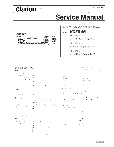


                                                                        Service Manual
                                                                                      AM/FM DVD/VCD/CD/MP3 Player

                                                                                      Model
                                                                                                  (PE-2630K-D)
                                                                                                  (for OCEANIA / Region No. "4")

                                                                                                  (PE-2630K-E)
                                                                                                  (for ASIA / Region No. "3")
                                                                                                  (PE-2630K-F)
                                                                                                  (for KOREA / Region No. "3")


                                                                                    Sector structure:        CD-ROM mode 1, mode 2 - form 1
SPECIFICATIONS
                                                                                                             (Automatic distinction)
FM tuner section
                                                                                    Logic format:            ISO9660 level 1,2,3,/JOLIET/ROMEO
Frequency range:           87.0MHz to 108.0MHz
                                                                                    Folder structure:        8 classes
Usable sensitivity:        9dBf
                                                                                    Number of folders:       Maximum of 255
50dB quieting sensitivity: 15dBf
                                                                                    Number of files:         Maximum of 500
Alternate channel selectivity:
                                                                                                             (Up to per 255 one folder)
                           70dB
                                                                                    File name:               128byte
Stereo separation:         35dB(1kHz)
                                                                                    Folder name:             Maximum of 128byte
Frequency response:        30Hz to 15kHz(+3/-3dB)

                                                                                    Audio section
AM tuner section
                                                                                    Maximum power output:    208W(52W x 4 ch)
Frequency range:           531kHz to 1629kHz
                                                                                    Continuous average power output:
Usable sensitivity:        25uV
                                                                                                             17W x 4(20Hz to 20kHz, 1%, 4 ohm)
                                                                                    Bass control action:     +16dB, -12dB(50Hz/80Hz/20Hz)
DVD player section
                                                                                    Table control action:    +12/-12dB(8kHz/12kHz)
System:                    Digital versatile disc system with CDDA
                                                                                    Line output level:       1.5V(CD 1kHz)
                           capable
Usable discs:              DVD video disc, Video CD, Compact disc
                                                                                    General
Frequency response:        20Hz to 20kHz(+1/-1dB)
                                                                                    Power supply voltage:    14.4V DC(10.8 to 15.6V allowable)
Signal to noise ratio:     90dB
                                                                                    Ground:                  Negative
Distortion:                 0.02%
                                                                                    Current consumption:     Less than 15A, 3A
Channel separation:        80dB
                                                                                    Speaker impedance:       4 ohm(4 ohm to 8 ohm allowable)
Analog audio output:       1.5Vrms
                                                                                    Dimensions(mm):          Main unit
                                                                                                             178(W) x 50(H) x 160(D)
MP3 section
                                                                                                             Remote control unit
MP3 decording:             MPEG-1; Audio layer 3
                                                                                                             54(W) x 155(H) x 27(D)
Sampling rate:             MPEG-1; 32kHz, 44.1kHz, 48kHz
                                                                                    Weight:                  Main unit 1.8kg
                           MPEG-2; 16kHz, 22.05kHz, 24kHz
                                                                                                             Remote control unit 100g
                           MPEG-2.5; 8kHz, 11.025kHz, 12kHz
                                                                                                             (including battery)
Bit rate:                  MPEG-1; 32k to 320kbps/VBR
                           MPEG-2; 8k to 160kbps/VBR
                           MPEG-2.5; 8k to 160kbps/VBR


                                                                                                                                                VXZ646
                                                                         -1-
COMPONENTS                                                               To engineers in charge of repair or inspe-
PE-2630K-D,K-E,K-F                                                       ction of our products.
  1.     Main unit                           -----------      1          Before repair or inspection, make sure to follow the in-
  2.     Remote controller                 RCB-166-200        1          structions so that customers and Engineers in charge
  3.     Battery(SUM-3)                     -----------       2          of repair or inspection can avoid suffering any risk or
  4.     Mounting bracket(straight)        300-4976-00        1          injury.
  5.     Mounting bracket(loop)            300-7742-00        1          1. Use specified parts.
  6.     DCP case                          335-6035-20        1             The system uses parts with special safety features against fire
  7.     Outer escutcheon                  370-6084-02        1             and voltage. Use only parts with equivalent characteristics when
  8.     Extension lead                    854-6349-50        1             replacing them.
  9.     Parts bag                          -----------       1             The use of unspecified parts shall be regarded as remodeling for
  9-1.   Removal key                       331-2497-00        2             which we shall not be liable. The onus of product liability (PL) sh-
  9-2.   Screw(M5 x 8)                     716-0496-01        1             all not be our responsibility in cases where an accident or failure
  9-3.   Lead holder                       335-0833-01        2             is as a result of unspecified parts being used.
  10.    Parts bag                           -----------      1          2. Place the parts and wiring back in their original positions after re-
  10-1. Ferrite core(small)                060-8041-00        1             placement or re-wiring.
  10-2. Ferrite core(large)                060-8043-00        2             For proper circuit construction, use of insulation tubes, bonding,
                                                                            gaps to PWB, etc, is involved. The wiring connection and routing
NOTES                                                                       to the PWB are specially planned using clamps to keep away
* Use a CeNET extension cable that is less than 20m in length.              from heated and high voltage parts. Ensure that they are placed
* This DVD video player can play the following discs.                       back in their original positions after repair or inspection.
                                                                            If extended damage is caused due to negligence during repair,
           R                                                                the legal responsibility shall be with the repairing company.
  Note: When you play a CD Extra disc, only the first session will be    3. Check for safety after repair.
         recognized.                                                        Check that the screws, parts and wires are put back securely in
* This player can play CD-R/CD-RW discs previously recorded in              their original position after repair. Ensure for safety reasons there
  music CD format or video CD format.                                       is no possibility of secondary ploblems around the repaired spots.
* This unit can playback CD-R/CD-RW discs on which MP3 music                If extended damage is caused due to negligence of repair, the
  data have been recorded.                                                  legal responsibility shall be with the repairing company.
* This DVD video player cannot playback DVD-R, DVD-RAM, Pho-             4. Caution in removal and making wiring connection to the parts for
  to CDs, etc.                                                              the automobile.
  Note: It may also not be possible to playback CDs recorded on a           Disconnect the battery terminal after turning the ignition key off.
         CD-R unit and CD-RW unit.                                          If wrong wiring connections are made with the battery connected,
* The DVD video system assigns a region number to DVD video                 a short circuit and/or fire may occur.
  players and DVD discs by sales area. This player can play "ALL"           If extensive damage is caused due to negligence of repair, the
  and "3" or "4" (and those inclusive). The DVD video region num-           legal responsibility shall be with the repairing company.
  ber is marked on the disc jacketas shown.                              5. Cautions regarding chips.
                       3                                                    Do not reuse removed chips even when no abnormality is obser-
  ALL     3      4         4
                               6                                            ved in their appearance. Always replace them with new ones.
* This product incorporates copyright protection technology that is         (The chip parts include resistors, capacitors, diodes, transistors,
  protected by method claims of certain U.S. patents and other int-         etc). The negative pole of tantalum capacitors is highly suscepti-
  ellectual property rights owned by Macrovision Corporation and            ble to heat, so use special care when replacing them and check
  other rights owners. Use of this copyright protection tecnology           the operation afterwards.
  must be authorized by Macrovision Corporation, and is intended         6. Cautions in handling flexible PWB
  for home and other limited viewing uses only unless otherwise au-         Before working with a soldering iron, make sure that the iron tip
  thorized by Macrovision Corporation. Reverse engineering or dis-          temperature is around 270 C. Take care not to apply the iron tip
  assembly is prohibited.                                                   repeatedly(more than three times) to the same patterns. Also ta-
* Manufactured under license from Dolby Laboratories.                       ke care not to apply the tip with force.
  "Dolby" and the double-D symbol are trademarks of Dolby Labor-         7. Turn the unit OFF during disassembly and parts replacement.
  atories.                                                                  Recheck all work before you apply power to the unit.
* "DTS" and "DTS Digital Surround" are registered trademarks of          8. Cautions in checking that the optical pickup lights up.
  Digital Theater Systems, Inc. Copyright 1996, 2003 Digital Theater        The laser is focused on the disc reflection surface through the
  Systems, Inc. All Rights Reserved.                                        lens of the optical pickup. When checking that the laser optical
* When the mechanism assy (HBS-523-100) of DVD mechanism                    diode lights up, keep your eyes more than 30cms away from the
  (slide mechanism) used for this model is replaced, it is necessary        lens. Prolonged viewing of the laser within 30cms may damage
  to check playback. Please refer to page 13 for details.                   your eyesight.
* We cannot supply PWB with component parts in principle. When            9. Cautions in handling the optical pickup
  a circuit on PWB has failure, please repair it by component parts         The laser diode of the optical pickup can be damaged by electr-
  base. Parts which are not mentioned in service manual are not             ostatic charge caused by your clothes and body. Make sure to
  supplied.                                                                 avoid electrostatic charges on your clothes or body, or discharge
* Specifications and design are subject to change without notice for        static electricity before handling the optical pickup.
  further improvement.

 VXZ646
                                                                        -2-
9-1. Laser diode
                                                                               SETTING THE CLOCK
     The laser diode terminals are shorted for transportation in order
                                                                               1. Press the [A] button to switch to the adjustment selection display.
     to prevent electrostatic damage. After replacement, open the
                                                                               2. Press the [      ] or [      ] button to select "CLOCK E".
     shorted circuit.
                                                                               3. Press the [        ] button.
     When removing the pickup from the mechanism, short the ter-
                                                                               4. Press the [     ] or [     ] button to select the hour or the minute.
     minals by soldering them to prevent this damage.
                                                                               5. Turn the [ROTARY] knob clockwise or counterclockwise to set
9-2. Actuator
                                                                                  the correct time.
     The actuator has a powerful magnetic circuit. If a magnetic
                                                                                  * The clock is displayed in 12-hour format.
     material is put close to it. Its characteristics will change.
                                                                               6. Press the [        ] button to store the time into memory.
     Ensure that not foreign substances enter through the ventilati-
                                                                               7. Press the [A] button to return to the previous mode.
     on slots in the cover.
9-3. Cleaning the lens                                                         * You cannot set the clock when it is displayed with only the ignition
     Dust on the optical lens affects performance.                               on. If you drain or remove the car's battery or take out this unit,
     To clean the lens, apply a small amount of isopropyl alcohol to             the clock is reset. While setting the clock, if another button or ope-
     lens paper and wipe the lens gently.                                       ration is selected, the clock set mode is canceled.


CAUTIONS                                                                       ABOUT THE 2-ZONE FUNCTION
Use of controls, adjustments or performance of procedures other                The 2-ZONE function is a function that outputs separate sounds
than those specified herein, may result in hazardous radiation exp-            from the MAIN zone and SUB zone by simultaneously operating two
osure.                                                                         sources in the one center unit, thereby allowing plural listeners to
The COMPACT DISC player and MINI DISC player should not be                     enjoy separate music sources. This unit can control its internal sour-
adjusted or repaired by anyone except properly qualified service               ces (radio, DVD, etc.) to play back them, and further, can simultane-
personnel.                                                                     ously play back sources from external equipment connected via
                                                                               CeNET (for instance, CD changers etc.). The sources of the MAIN
                                                                               zone are played back from the speakers of the vehicle side, and
SYSTEM CHECK                                                                   those of the SUB zone are from the headphone systems
The first time this unit is turned on after the wire connections are
                                                                               (WH104/WH204).
completed, it must be checked what equipment is connected. When
the power is turned on, "SYSTEM CHK" and "Push POWER" appe-                    * Except AUX, the MAIN and SUB zones cannot simultaneously use
ar in the display alternately, so press the [FNC] button. The system            sources inside this unit. Also, external equipment connected via
check starts within the unit. When the system check is complete,                CeNET cannot simultaneously be used.
press the [FNC] button again.                                                  * The TV mode while the 2-ZONE function is tuned on is forced to
                                                                                change to "VTR playback".
                                                                               * The ISR function cannot be operated when the 2-ZONE function is
                                                                                turned on.
                                                                               * The Audio mode and Z-enhancer function cannot be set for the
                                                                                sources of the SUB zone.


TROUBLESHOOTING
                Problem                      Cause                                   Measure

  General       Nothing happens when         The microprocessor has malfun-          Turn off the power, then press the [RELEASE] button and
                buttons are pressd.          ction due to noise, etc.                remove the DCP. Press the reset button for about 2 seconds
                Display is not accurate.                                             with a thin rod.


                                                                                                                      Reset button

  DVD           Audio and video are not      MP3 files are absent in a disc.         Write MP3 files onto the disc properly.
  (CD/MP3)      output.
                                             Files are not recognized as an MP3      Use MP3 files encoded properly.
                                             file.

                                             File system is not correct.             Use ISO9660 level 1, 2 or JOLIET or Romeo file system.
                Sound is cut or slipped.     MP3 files are not encoded properly. Use MP3 files encoded properly.
                Noise is generated or
                noise is mixed with sou-
                nd.

                Wrong filename               File system is not correct.             Use ISO9660 level 1, 2 or JOLIET or Romeo file system.


                                                                                                                                           VXZ646
                                                                    -3-
ERROR DISPLAYS
If an error occurs, one of the following displays is displayed. Take the measures described below to eliminate the problem.
              Error display    Cause                                                    Measure
              ERROR 2          The failure of a DVD/CD itself considered.               This is a failure of DVD deck's mechanism.
              ERROR 3          A DVD/CD cannot be played due to scratches, etc.         Replace with a non-scratched, non-warped disc.
                               A DVD/CD cannot be played due to the defective
 DVD                           pick-up part.
 (CD/MP3)                      The disc is placed up side down.
              ERROR 6          A DISC inside a DVD/CD cannot be played because          Eject the disc then reload it properly.
                               it is loaded upside-down.
              ERROR R          Disc region code incorrect.                              Use a disc with the correct region code.
              ERROR P          The view is limited.                                     Release the view limitation or change the parental
                                                                                        level.
              ERROR 2          A CD inside the CD changer is not loaded.                This is a failure of CD changer's mechanism.
              ERROR 3          A CD inside the CD changer cannot be played due          Replace with a non-scratched, non-warped disc.
 CD
                               to scratches, etc.
 changer
              ERROR 6          A CD inside the CD changer cannot be played be-          Eject the disc then reload it properly.
                               cause it is loaded upside-down.
              ERROR 2          A DISC inside the DVD changer cannot be played.          This is a failure of DVD mechanism.
              ERROR 3          A DISC cannot be played due to scratches, etc.           Retry or replace with a non-scratched, non-warped
                                                                                        disc.
 DVD
              ERROR 6          A DISC inside the DVD changer cannot be played           Eject the disc then reload it properly.
 changer
                               because it is loaded upside-down.
              ERROR P          Parental level error                                     Set the correct Parental level.
              ERROR R          Region code error                                        Eject the disc and replace correct region code disc.
              AMP GUARD        The speaker protection circuit is operating.             Turn down sound volume. Function can also be resto-
                               During this operation, if any volume operation is        red by turning the power off and on again.
 General
                               performed, the display shows "AMP GUARD".                (Speaker volume is reduced automatically when the
                                                                                        speaker protection circuit operates).

* If an error display other than the ones described above appears, press the reset button. If the problem persists, turn off the power and
  consult your store of purchase.


BLOCK DIAGRAM
DVD mechanism section
                                                MAIN PWB
                                                                                    IC505
                                                                                  16M DRAM
                                                                                  MSM56V16160F

            PICKUP 4.74XL
                                                      IC101                        IC301
            LASER DIODE                                                     SERNO/DATA/IF(ATAPI)            ATAPI I/F
                                                      RF-AMP                                                                 HOST CPU
             I/V AMP,                                                       PROCESSOR
            PHOTO DIODE                               TA1363AF              TC94A11F

             FOCUSING &
             TRACKING
             ACTUATOR


                                                     IC204
               SLED                              ACTUATOR &
               MOTOR                             MOTOR DRIVER
                                                      BD7902CFS


              SPINDLE                                                                                                        HOST CPU
                                                                                    IC501
              MOTOR                                                                                                          9V, 5V, 3.3V
                                                                                   MECHE.
                                                                                   MAIN CPU
                                                                                  TMP91CW12AF


              LOADING
              MOTOR
             SMA-192-100


 VXZ646
                                                                            -4-
                                       Main section


                             DVD PWB


-5-
                 DVD MECHANISM


           SWITCH PWB


  VXZ646
EXPLANATION OF IC                                                                                                     051-5446-08            BD4843G                     Precision Vlotage Detector 4.3V

051-2050-01           LA47532-S                                   Quad Bridge Power Amplifiers                                                                           VDD


                          AU X IN 1                                                                                    OUTPUT 1                    5 N.C.                                                    Vout
                                                                                    2 2 GND                            VDD             2
       St and b y (H = Amp ON ) 4
                                                                                    3 2 OUT -                          GND             3           4 N.C.
                              VCC 6                                            +    5 2 OUT +
                                                                                                                                                                  Vref
                  R i p p l e F i l te r 10                                         7 1 OUT -
                               1 IN 11                                              8 1 GND
                                                                               +                                                                                          GND
                               2 IN 12                                              9 1 OUT +

                      P R E GN D 13
                                                                                                                      Terminal description
                               4 IN 14                                              17 3 OUT +                         pin 1: OUTPUT                        : N channel open drain output, positive logic.
                                                                               +
                               3 IN 15                                              18 3 GND                           pin 2: VDD                           : Positive supply voltage.
                     ON ti me C 16                                                  19 3 OUT -
                                                                                                                       pin 3: GND                           : Ground.
                              V C C 20                                         +    21 4 OUT +                         pin 4: NC                            : Not in use.
                                                                                    23 4 OUT -
         MU T E (L = Mu te ON ) 22                                                                                     pin 5: NC                            : Not in use.
                                                                                    24 4 GND
             (n e g a ti v e l o g i c ) 25           Off set Det ect
                                                                                                                      051-5834-90            uPC5701GR-028-8JG                            Variable      Fc    LPF


051-3297-00           BA4916                                                       Power Supply System
                                                                                                                                       D EC 1 1                                         20 1st LPF C2
                                                                                                                                                      LOGIC          LPF 1
                                                                                                                                       D EC 2 2                                         19 1st OUT
                                                            VDD-0.7V               3 COMP OUT
                                                            VDD DET                1 RESET OUT                                          GND 3                                           18 1st LPF C1
                ACC IN 4
                                                              5.7V                                                               1st IN LPF 4                                           17 VCC
                    VCC 9                                                          5 VDD OUT
                                                            Stabilized
                Ground 12                                                                                                        1st IN THR 5                                           16 N.C.
                                                            VCC-0.5V               2 EXT OUT
                                                               9V                                                                       TEST 6                                          15 2nd LPF C2
                                     Controller


                                                                                                     See the table


                                                                                   6 AUDIO OUT
                                                            Stabilized
                Control 8                                                                                                                                            LPF 2
                                                               8V                                                                2nd IN LPF 7                                           14 2nd OUT
                                                                                   7 CD OUT
                                                            Stabilized
                                                               10V                                                              2nd IN THR 8                                            13 2nd LPF C1
            ILL Voltage                                                            10 ILLUMI OUT
                        11                                  Adjustable
                 Adjust                                                                                                                 GND 9                                           12 VCC


                                                                                                                                  Iref adjust 10                                        11 1/2 VCC
Table 1. Output Control
  CTRL                                               EXT            AUDIO               CD           LIM
                                                                                                                      Fc Table
    in                                                out             out               out           out
  (pin 8)                                           (pin 2)         (pin 6)           (pin 7)      (pin 10)                Fc                                                  DEC 1(pin 1)       DEC 2(pin 2)
   L                                                  off                off            off          off                   Through                                                  0                   0
   M                                               Vcc-0.5V              9V             off         10V                     120Hz                                                   0                   1
   H                                               Vcc-0.5V              9V             8V          10V                         80Hz                                                1                   0
         0.0V < L < 1.5V,                         2.0V < M < 3.0V,                 4.1V < H < 5.9V                              50Hz                                                1                   1


051-3333-00           NJM2396F05                              Positive Voltage Regurator (5.0V)
                                                                                                                      051-9320-30            HY57V161610DTC-7I
                                                                                                                                                 2 Banks x 512K x 16 bit Synchronous DRAM

                                                     4 Control input ( ON = H or Open )                               1.Terminal Description
                                                     3 Ground                                                          pin 1: VDD                           : - : Positive supply voltage.
                                                     2 Power output
                                                                                                                       pin 2: DQ 0                          :I/O: Data signal input/output.
                                                     1 Power input
                                                                                                                       pin 3: DQ 1                          :I/O: Data signal input/output.
                                                                                                                       pin 4: VSS                           : - : Negative supply voltage.
051-3334-00           NJM2396F09                              Positive Voltage Regurator (9.0V)                        pin 5: DQ 2                          :I/O: Data signal input/output.
                                                                                                                       pin 6: DQ 3                          :I/O: Data signal input/output.
                                                                                                                       pin 7: VDD                           : - : Positive supply voltage.
                                                     4 Control input ( ON = H or Open )                                pin 8: DQ 4                          :I/O: Data signal input/output.
                                                     3 Ground                                                          pin 9: DQ 5                          :I/O: Data signal input/output.
                                                     2 Power output                                                    pin 10: VSS                          : - : Negative supply voltage.
                                                     1 Power input
                                                                                                                       pin 11: DQ 6                         :I/O: Data signal input/output.
                                                                                                                       pin 12: DQ 7                         :I/O: Data signal input/output.
                                                                                                                       pin 13: VDD                          : - : Positive supply voltage.
051-9406-28           BR24L01AF                                                    128 x 8 bit EEP-ROM
                                                                                                                       pin 14: L DQM                        : IN : Lower DQM. Input/output masking signal
                                                                                                                                                                   input.
1. Terminal Description
 pin 1: Slave add set 0              : IN : Slave address setting input.                                               pin      15: WE                      : IN : Write enable signal input.
 pin 2: Slave add set 1              : IN : Slave address setting input.                                               pin      16: CAS                     : IN : Column address strobe input.
 pin 3: Slave add set 2              : IN : Slave address setting input.                                               pin      17: RAS                     : IN : Raw address strobe input.
 pin 4: GND                          : - : Ground.                                                                     pin      18: CS IN                   : IN : The chip select command input.
 pin 5: S DA                         :I/O: The serial data input/output.                                               pin      19: A 11                    : IN : Address signal input.
 pin 6: SCK                          : IN : The clock pulse input.                                                     pin      20: A 10                    : IN : Address signal input.
 pin 7: Write Protect                : IN : Write protect signal input.                                                pin      21: A 0                     : IN : Address signal input.
 pin 8: VCC                          : - : Positive supply voltage.                                                    pin      22: A 1                     : IN : Address signal input.
                                                                                                                       pin      23: A 2                     : IN : Address signal input.
 VXZ646
                                                                                                                     -6-
pin   24: A 3           : IN : Address signal input.                      pin   45: SEG 45         : O : The   segment   signal   output.
pin   25: VDD           : - : Positive supply voltage.                    pin   46: SEG 46         : O : The   segment   signal   output.
pin   26: VSS           : - : Negative supply voltage.                    pin   47: SEG 47         : O : The   segment   signal   output.
pin   27: A 4           : IN : Address signal input.                      pin   48: SEG 48         : O : The   segment   signal   output.
pin   28: A 5           : IN : Address signal input.                      pin   49: SEG 49         : O : The   segment   signal   output.
pin   29: A 6           : IN : Address signal input.                      pin   50: SEG 50         : O : The   segment   signal   output.
pin   30: A 7           : IN : Address signal input.                      pin   51: SEG 51         : O : The   segment   signal   output.
pin   31: A 8           : IN : Address signal input.                      pin   52: SEG 52         : O : The   segment   signal   output.
pin   32: A 9           : IN : Address signal input.                      pin   53: SEG 53         : O : The   segment   signal   output.
pin   33: NU            : - : Not in use.                                 pin   54: SEG 54         : O : The   segment   signal   output.
pin   34: CKE           : IN : Clock enable signal input.                 pin   55: SEG 55         : O : The   segment   signal   output.
pin   35: CLK           : IN : The clock pulse input.                     pin   56: SEG 56         : O : The   segment   signal   output.
pin   36: U DQM         : IN : Upper DQM. Input/output masking signal     pin   57: SEG 57         : O : The   segment   signal   output.
                               input.                                     pin   58: SEG 58         : O : The   segment   signal   output.
pin   37: NU            : - : Not in use.                                 pin   59: SEG 59         : O : The   segment   signal   output.
pin   38: VDD           : - : Positive supply voltage.                    pin   60: SEG 60         : O : The   segment   signal   output.
pin   39: DQ 8          :I/O: Data signal input/output.                   pin   61: SEG 61         : O : The   segment   signal   output.
pin   40: DQ 9          :I/O: Data signal input/output.                   pin   62: SEG 62         : O : The   segment   signal   output.
pin   41: VSS           : - : Negative supply voltage.                    pin   63: SEG 63         : O : The   segment   signal   output.
pin   42: DQ 10         :I/O: Data signal input/output.                   pin   64: SEG 64         : O : The   segment   signal   output.
pin   43: DQ 11         :I/O: Data signal input/output.                   pin   65: SEG 65         : O : The   segment   signal   output.
pin   44: VDD           : - : Positive supply voltage.                    pin   66: COMMON 1       : O : The   common    signal   output.
pin   45: DQ 12         :I/O: Data signal input/output.                   pin   67: COMMON 2       : O : The   common    signal   output.
pin   46: DQ 13         :I/O: Data signal input/output.                   pin 68: COMMON 3      : O : The common signal output.
pin   47: VSS           : - : Negative supply voltage.                    pin 69: COMMON 4      : O : The common signal output.
pin   48: DQ 14         :I/O: Data signal input/output.                   pin 70: COMMON 5      : O : The common signal output.
pin   49: DQ 15         :I/O: Data signal input/output.                   pin 71: COMMON 6      : O : The common signal output.
pin   50: VSS           : - : Negative supply voltage.                    pin 72: COMMON 7      : O : The common signal output.
                                                                          pin 73: COMMON 8      : O : The common signal output.
051-6073-00       NJU6538FG1                  LCD Driver with Key scan    pin 74: COMMON 9      : O : The common signal output.
pin    1: SEG    1      : O : The   segment   signal   output.            pin 75: COMMON 10     : O : The common signal output.
pin    2: SEG    2      : O : The   segment   signal   output.            pin 76: PO 0          : O : 128 steps PWM output.
pin    3: SEG    3      : O : The   segment   signal   output.            pin 77: PO 1          : O : 128 steps PWM output.
pin    4: SEG    4      : O : The   segment   signal   output.            pin 78: PO 2          : O : 128 steps PWM output.
pin    5: SEG    5      : O : The   segment   signal   output.            pin 79: KS OUT 0/PO 3 : O : Key scan output / 128 steps PWM output.
pin    6: SEG    6      : O : The   segment   signal   output.            pin 80: KS OUT 1      : O : Key scan output.
pin    7: SEG    7      : O : The   segment   signal   output.            pin 81: KS OUT 2      : O : Key scan output.
pin    8: SEG    8      : O : The   segment   signal   output.            pin 82: KS OUT 3      : O : Key scan output.
pin    9: SEG    9      : O : The   segment   signal   output.            pin 83: KS OUT 4      : O : Key scan output.
pin   10: SEG   10      : O : The   segment   signal   output.            pin 84: KS IN 0       : IN : Key scan input.
pin   11: SEG   11      : O : The   segment   signal   output.            pin 85: KS IN 1       : IN : Key scan input.
pin   12: SEG   12      : O : The   segment   signal   output.            pin 86: KS IN 2       : IN : Key scan input.
pin   13: SEG   13      : O : The   segment   signal   output.            pin 87: KS IN 3       : IN : Key scan input.
pin   14: SEG   14      : O : The   segment   signal   output.            pin 88: KS IN 4       : IN : Key scan input.
pin   15: SEG   15      : O : The   segment   signal   output.            pin 89: VDD           : - : Positive supply voltage.
pin   16: SEG   16      : O : The   segment   signal   output.            pin 90: V LCD 1       : - : The driving voltage for the LCD.
pin   17: SEG   17      : O : The   segment   signal   output.            pin 91: V LCD 2       : - : The bias voltage for the LCD.
pin   18: SEG   18      : O : The   segment   signal   output.            pin 92: V0            : - : The bias voltage for the LCD.
pin   19: SEG   19      : O : The   segment   signal   output.            pin 93: V1            : - : The bias voltage for the LCD.
pin   20: SEG   20      : O : The   segment   signal   output.            pin 94: V2            : - : The bias voltage for the LCD.
pin   21: SEG   21      : O : The   segment   signal   output.            pin 95: VSS           : - : Negative supply voltage.
pin   22: SEG   22      : O : The   segment   signal   output.            pin 96: OSC           : - : For oscillating.
pin   23: SEG   23      : O : The   segment   signal   output.            pin 97: RESET         : IN : Reset signal input.
pin   24: SEG   24      : O : The   segment   signal   output.            pin 98: CE            : IN : Chip enable signal input.
pin   25: SEG   25      : O : The   segment   signal   output.            pin 99: SCK           : IN : The clock pulse input.
pin   26: SEG   26      : O : The   segment   signal   output.            pin100: S DATA        :I/O: Serial data input/output.
pin   27: SEG   27      : O : The   segment   signal   output.
pin   28: SEG   28      : O : The   segment   signal   output.            052-6058-10     MR27V802D-A6TPZ010              8M bit One Time PROM
pin   29: SEG   29      : O : The   segment   signal   output.
                                                                          1.Terminal Description
pin   30: SEG   30      : O : The   segment   signal   output.             pin 1: NU               : - : Not in use.
pin   31: SEG   31      : O : The   segment   signal   output.             pin 2: A 18             : IN : The address input.
pin   32: SEG   32      : O : The   segment   signal   output.             pin 3: A 17             : IN : The address input.
pin   33: SEG   33      : O : The   segment   signal   output.             pin 4: A 7              : IN : The address input.
pin   34: SEG   34      : O : The   segment   signal   output.             pin 5: A 6              : IN : The address input.
pin   35: SEG   35      : O : The   segment   signal   output.             pin 6: A 5              : IN : The address input.
pin   36: SEG   36      : O : The   segment   signal   output.             pin 7: A 4              : IN : The address input.
pin   37: SEG   37      : O : The   segment   signal   output.             pin 8: A 3              : IN : The address input.
pin   38: SEG   38      : O : The   segment   signal   output.             pin 9: A 2              : IN : The address input.
pin   39: SEG   39      : O : The   segment   signal   output.             pin 10: A 1             : IN : The address input.
pin   40: SEG   40      : O : The   segment   signal   output.             pin 11: A 0             : IN : The address input.
pin   41: SEG   41      : O : The   segment   signal   output.             pin 12: Chip enable     : IN : Chip enable signal input.
pin   42: SEG   42      : O : The   segment   signal   output.            pin 13: VSS              : - : Ground.
pin   43: SEG   43      : O : The   segment   signal   output.
                                                                          pin 14: Output enable    : IN : Output enable signal input.
pin   44: SEG   44      : O : The   segment   signal   output.
                                                                          pin 15: D 0              : O : The data output.
                                                                                                                                            VXZ646
                                                                    -7-
pin   16: D 8            : O : The data output.                               pin 45: PLL DI      : IN : Serial data input from the PLL IC.
pin   17: D 1            : O : The data output.                               pin 46: ST / SD     : IN : At receiving the FM station, this port de-
pin   18: D 9            : O : The data output.                                                          tects the stereo signal. At seeking or scan-
pin   19: D 2            : O : The data output.                                                          ning, this port detects the station detection
                                                                                                         signal.
pin   20: D 10           : O : The data output.
                                                                              pin 47: SYS ACC     : O : ACC detect signal output.
pin   21: D 3            : O : The data output.
                                                                              pin 48: FIL CONT 2  : O : The cut off frequency control signal output
pin   22: D 11           : O : The data output.
                                                                                                         to the filter. Refer Table-1.
pin   23: VCC            : - : Positive supply voltage.
                                                                              pin 49: FIL CONT 1  : O : The cut off frequency control signal output
pin   24: D 4            : O : The data output.                                                          to the filter. Refer Table-1.
pin   25: D 12           : O : The data output.                               pin 50: NU          : IN : Not in use.
pin   26: D 5            : O : The data output.                               pin 51: NU          : IN : Not in use.
pin   27: D 13           : O : The data output.                               pin 52: CTRL        : O : Power supply ON signal output.
pin   28: D 6            : O : The data output.                               pin 53: NU          : IN : Not in use.
pin   29: D 14           : O : The data output.                               pin 54: E VOL CLK   : O : The clock pulse output to the volume IC.
pin   30: D 7            : O : The data output.                               pin 55: E VOL DATA  : O : The serial data output to the volume IC.
pin   31: D 15 / A -1    :I/O: The data output. / The address input.          pin 56: INT AMP REM : O : ON signal output to the internal Amplifier.
pin   32: VSS            : - : Ground.                                        pin 57: EXT AMP REM : O : ON signal output to the external Amplifier.
pin   33: BYTE           : IN : 8bit/16bit selection.                         pin 58: AMP MUTE    : O : Muting signal output to the Audio Power
pin   34: A 16           : IN : The address input.                                                       Amplifier.
pin   35: A 15           : IN : The address input.                            pin 59: NU          : IN : Not in use.
pin   36: A 14           : IN : The address input.                            pin 60: VCC         : - : Positive supply voltage.
pin   37: A 13           : IN : The address input.                            pin 61: NU          : IN : Not in use.
pin   38: A 12           : IN : The address input.                            pin 62: GND         : - : Ground.
pin   39: A 11           : IN : The address input.                            pin 63: LINE SYS MU : O : The system muting command output.
pin   40: A 10           : IN : The address input.                            pin 64: NAVI MUTE   : O : Muting signal output to suppress the noise
pin   41: A 9            : IN : The address input.                                                       without Navigation sound interrupting.
pin   42: A 8            : IN : The address input.                            pin 65: 2-zone Mute : O : 2-zone muting control.
pin   43: NU             : - : Not in use.                                    pin 66: NU          : IN : Not in use.
pin   44: NU             : - : Not in use.                                    pin 67: 5V REM      : O : ON signal output to the 5V power supply.
                                                                              pin 68: KEY ILL REM : O : Key illumination ON signal output.
052-3392-01     M30622MEP-168GP                      System Controller        pin 69: AUT ANT REM : O : Motor Antenna control signal output.
                                                                              pin 70: DISP+B REM  : O : The power supply control signal output for
[NOTE] 052-3392-01 is compatible with 052-3392-00                                                        the LCD driver.
Terminal Description                                                          pin 71: NU          : IN : Not in use.
 pin 1: H-DVD ST       : IN : A communication port for H-DVD mechanism.       pin 72: NU          : IN : Not in use.
 pin 2: REMOCON        : IN : Remote controller signal input terminal.        pin 73: OFFSET DET : IN : The emergency signal input from the pow-
 pin 3: DP DT          : O : The communication port for DVD proces-                                      er IC.
                              sor IC.                                         pin 74: ILL DET     : IN : Illumination ON signal input.
 pin 4: NU             : IN : Not in use.                                     pin 75: NU          : IN : Not in use.
 pin 5: DP CK          : O : The communication port for DVD proces-           pin 76: DVD ON 1    : O : DVD ON signal output.
                              sor IC.                                         pin 77: DVD ON 2    : O : DVD ON signal output.
 pin 6: BYTE           : IN : The data length selection(8bit/16bit).          pin 78: PHONE INT   : IN : The telephone interrupt signal input.
 pin 7: CN VSS         : IN : Connect to VSS.                                 pin 79: INIT 1      : IN : The initial setting input.
 pin 8: JOG CW         : IN : Jog key signal input.                           pin 80: INIT 2      : IN : The initial setting input.
 pin 9: JOG CCW        : IN : Jog key signal input.                           pin 81: REG 1       : IN : Initial setting terminal.
 pin 10: RESET         : IN : Reset signal input.                             pin 82: REG 2       : IN : Initial setting terminal.
 pin 11: X out         : O : Crystal connection.                              pin 83: REG 3       : IN : Initial setting terminal.
 pin 12: VSS           : - : Negative supply voltage.                         pin 84: VIDEO MUTE : O : The video mute signal output.
 pin 13: X IN          : IN : Crystal connection.                             pin 85: KEY A/D     : IN : The input terminal of the internal ADC for
 pin 14: VCC           : - : Positive supply voltage.                                                    key judgement.
 pin 15: NMI           : IN : Connect to VDD.                                 pin 86: EJECT out   : O : Eject command output.
 pin 16: ACC DET       : IN : ACC detection signal input.                     pin 87: DVD ACC     : O : Wakeup signal output to DVD mechanism
 pin 17: BU DET        : IN : Backup detection signal input.                                             controller.
 pin 18: KEY INT       : IN : Key interrupting signal input.                  pin 88: SYS P1      : IN : System power 1 control signal input.
 pin 19: 27pin connect : IN : Connect to 27pin.                               pin 89: NU          : IN : Not in use.
 pin 20: NU            : IN : Not in use.                                     pin 90: NU          : IN : Not in use.
 pin 21: NU            : IN : Not in use.                                     pin 91: ES RST      : O : The reset pulse output to DVD processor IC.
 pin 22: BEEP          : O : Beep out.                                        pin 92: NU          : IN : Not in use.
 pin 23: TIME BASE     : IN : Time base pulse input.                          pin 93: FE RST      : O : The reset pulse output to H-DVD mecha-
 pin 24: LCD CS        : O : Chip select signal output to the LCD driver.                                nism controller.
 pin 25: LCDSISO       :I/O: The communication port for LCD controller.       pin 94: A VSS       : - : Analog ground.
 pin 26: LCD CLK       : O : The clock pulse output to the LCD driver.        pin 95: NU          : IN : Not in use.
 pin 27: IE BUS RX     : IN : IE Bus serial data input.                       pin 96: Vref        : - : Reference voltage.
 pin 28: IE BUS TX     : O : IE Bus serial data output.                       pin 97: A VCC       : - : Positive supply voltage for the internal an-
                                                                                                         alog section.
 pin 29: EMULATOR TX : O : The serial data output to the emulator.
                                                                              pin 98: NU          : IN : Not in use.
 pin 30: EMULATOR RX : IN : The serial data input from the emulator.
                                                                              pin 99: NU          : IN : Not in use.
 pin 31: FLASH MODE : IN : The flash memory mode setting input.
                                                                              pin100: NU          : IN : Not in use.
 pin 32: FLASH MODE : O : Not in use (open).
 pin 33: NU            : IN : Not in use.
 pin 34: ES DT         : IN : The communication port for DVD proces-         Table-1. Analog Mater IC uPC5701 control
                              sor IC.                                                                                  FIL_CONT 1      FIL_CONT 2
 pin 35: ES CK         : IN : The communication port for DVD proces-          Line out Signal                            (pin 49)        (pin 48)
                              sor IC.                                             Non Fader output                         L                L
 pin 36: NU            : O : Not in use.                                          Sub-Woofer 120Hz                         L                H
 pin 37: INIT 3        : IN : The initial setting input.                          Sub-Woofer 80Hz                          H                L
 pin 38: INIT 4        : IN : The initial setting input.                          Sub-Woofer 50Hz                          H                H
 pin 39: FLASH MODE : IN : The flash memory mode setting input.
 pin 40: NU            : IN : Not in use.
 pin 41: PLL DO        : O : Serial data output to the PLL IC.
 pin 42: PLL CE        : O : The chip enable signal output to the PLL IC.
 pin 43: PLL SCK       : O : The clock pulse output to the PLL IC.
 pin 44: FLASH MODE : IN : The flash memory mode setting input.


 VXZ646
                                                                            -8-
EXPLODED VIEW / PARTS LIST
DCP section

                                                                                                       1-23
                                                                                    1-22
                                                                         1-20
                                                                 1-48               1-24
                                                             1-53
                                                    1-14                                    1-47
                                                                                     1-51
                                                                  1-47                       1-50                               1-23
                         1
                                1-12        1-13           1-15                                                                        1-43        1-42
                                                                         1-49                                  1-24
                             1-11                                                                                                             1-45
                                                  1-29                              1-46                           1-41
                     1-10                                            1-16                                                                        1-44
                                                                                                               1-39     1-40
                      1-25                                                  1-29              1-47                                                       1-52
                                                                                                              1-38
             1-8                                                                                     1-21                                                         1-40
                                                                                                                                  1-40
1-5       1-6
                                                             1-17                                                                1-39
                                                                                                                                                1-40
                                                                                                                         1-37
 1-28                                                                                       1-19                                         1-39
                    1-9             1-27                                                                                                                  1-40
                                           1-26                                 1-18                                            1-38
                                                                                                                                                       1-39
                                                           1-27
       1-2                            1-9
                                                                                                                                       1-36
                                                     1-7                                                                 1-34 1-35
                   1-4
                                                                                                                 1-33
                                                     1-1                                                1-31 1-32


◦ Jabse Service Manual Search 2024 ◦ Jabse PravopisonTap.bg ◦ Other service manual resources online : FixyaeServiceinfo