Service Manuals, User Guides, Schematic Diagrams or docs for : panasonic LCD TH-42PY70FA th_42pz70ba_sim
<< Back | HomeMost service manuals and schematics are PDF files, so You will need Adobre Acrobat Reader to view : Acrobat Download Some of the files are DjVu format. Readers and resources available here : DjVu Resources
For the compressed files, most common are zip and rar. Please, extract files with Your favorite compression software ( WinZip, WinRAR ... ) before viewing. If a document has multiple parts, You should download all, before extracting.
Good luck. Repair on Your own risk. Make sure You know what You are doing.
Image preview - the first page of the document

>> Download th_42pz70ba_sim documenatation <<
Text preview - extract from the document
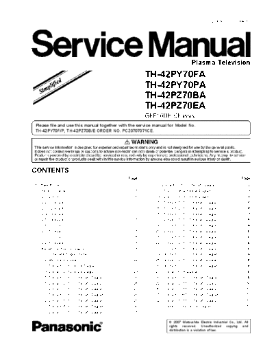
                                                                                           ORDER NO.PCZ0709093AE


                                                                                 Plasma Television
                                                     TH-42PY70FA
                                                     TH-42PY70PA
                                                     TH-42PZ70BA
                                                     TH-42PZ70EA
                                                     GPF10DE Chassis
Please file and use this manual together with the service manual for Model No.
TH-42PY70F/P, TH-42PZ70B/E ORDER NO. PCZ0707071CE.


CONTENTS
                                              Page                                                               Page
1 Different PCB                                  3       3.12. D-Board (8 of 8) Schematic Diagram                    32
2 Conductor Views                                5       3.13. C1 and C4-Board Block Diagram                         33
    2.1. D-Board                                 5       3.14. C2 and C3-Board Block Diagram                         34
    2.2. C1-Board                                8       3.15. C1-Board (1 of 3) Schematic Diagram                   35
    2.3. C2-Board                                9       3.16. C1-Board (2 of 3) Schematic Diagram                   36
    2.4. C3-Board                               10       3.17. C1-Board (3 of 3) Schematic Diagram                   37
    2.5. C4-Board                               11       3.18. C2-Board (1 of 3) Schematic Diagram                   38
    2.6. SC-Board                               12       3.19. C2-Board (2 of 3) Schematic Diagram                   39
    2.7. SU-Board                               15       3.20. C2-Board (3 of 3) Schematic Diagram                   40
    2.8. SD-Board                               16       3.21. C3-Board (1 of 3) Schematic Diagram                   41
    2.9. SS-Board                               17       3.22. C3-Board (2 of 3) Schematic Diagram                   42
3 Schematic and Block Diagram                   21       3.23. C3-Board (3 of 3) Schematic Diagram                   43
    3.1. Schematic Diagram Note                 21       3.24. C4-Board (1 of 3) Schematic Diagram                   44
    3.2. Main Block Diagram                     22       3.25. C4-Board (2 of 3) Schematic Diagram                   45
    3.3. D-Board (1 of 2) Block Diagram         23       3.26. C4-Board (3 of 3) Schematic Diagram                   46
    3.4. D-Board (2 of 2) Block Diagram         24       3.27. SC-Board Block Diagram                                47
    3.5. D-Board (1 of 8) Schematic Diagram     25       3.28. SC-Board (1 of 5) Schematic Diagram                   49
    3.6. D-Board (2 of 8) Schematic Diagram     26       3.29. SC-Board (2 of 5) Schematic Diagram                   50
    3.7. D-Board (3 of 8) Schematic Diagram     27       3.30. SC-Board (3 of 5) Schematic Diagram                   51
    3.8. D-Board (4 of 8) Schematic Diagram     28       3.31. SC-Board (4 of 5) Schematic Diagram                   52
    3.9. D-Board (5 of 8) Schematic Diagram     29       3.32. SC-Board (5 of 5) Schematic Diagram                   53
   3.10. D-Board (6 of 8) Schematic Diagram     30       3.33. SU and SD-Board Block Diagram                         54
   3.11. D-Board (7 of 8) Schematic Diagram     31
◦ Jabse Service Manual Search 2024 ◦ Jabse Pravopis ◦ onTap.bg ◦ Other service manual resources online : Fixya ◦ eServiceinfo