Service Manuals, User Guides, Schematic Diagrams or docs for : xerox notetaker memos 19790605_Definition_of_8086_Ports

<< Back | Home

Most service manuals and schematics are PDF files, so You will need Adobre Acrobat Reader to view : Acrobat Download Some of the files are DjVu format. Readers and resources available here : DjVu Resources
For the compressed files, most common are zip and rar. Please, extract files with Your favorite compression software ( WinZip, WinRAR ... ) before viewing. If a document has multiple parts, You should download all, before extracting.
Good luck. Repair on Your own risk. Make sure You know what You are doing.


Image preview - the first page of the document
19790605_Definition_of_8086_Ports


>> Download 19790605_Definition_of_8086_Ports documenatation <<

Text preview - extract from the document
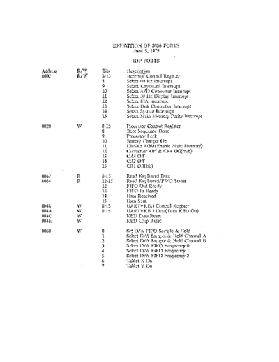
                        DEFINITION OF 8086 PORTS
                               June 5, 1979

                               lOP PORTS

Address   RAV   Bits        Description
0002      R/W   8-15        Interrupt Control Register
                8           Select 60 Hz Interrupt
                9           Se1ect Key Board Internlpt
                10          Select AID Converter Intcrfilpt
                11          Select 30 Hz Display Inte~rupt
                12          Select EIA Interrupt
                13          Select Disk Controller Interrupt
                14          Select System Interrupt
                15          Select wI ain Niemory Parity Interrupt

0020      'tV   8-15        Processor Control Register
                8           Boot Sequence Done
                9           Processor Lock
                10          Battery Charger On
                11          Disabic ROrvr(Enable Ivlain lvlcmury)
                12          Correction Off & CR4 Off(msb)
                13          CR30fr
                14          CR2 orr
                15          CR1 Off(lsb)

0042      R     8-15        Read Key Board Data
0044      R     12-15       Read KeyBoard/FIFO Status
                12          FIFO Out Ready
                13          FIFO In Ready
                14          Data Received
                15          Data Sent
0048      W     8-15        UART+- KBD Control Register
004A      W     8-15        UART +- KBD Data(Turn KBD On)
004C      W                 KI3D Data Reset
004E      W                 KBD Chip Reset

0060      \V    0           Set D/A FIFO Sample & Hold
                1           Select D/A Sample & Hold Channel A
                2           Select DI A Sample & Hold Channel B
                3           Select 01 A FIFO Frequency 0
                4           Select DI A FIFO Frequency 1
                5           Select DIA FIFO Frequency 2
                6           Tablet X On
                7           Tablet Y On
                                                                        2


Address   U/\V   Hits    Description
OOAO      W-     8-15    DataBus to PPI Interface PortA
OOAO      R      8-15    PPI Interface PortA to DataBus
00A2      'N     8-15    DataBus to PPI Interface PortB
00A2      R      8-15    PPI Interface PortB to DataBus
00A4      W      8-15    DataBus to PPI Interface PortC
00A4      R      8-15    PPI Interface PortC to Data Bus
                 8       Bit Set/Reset Flag(O=active)
                 9-11    Dant Care
                 12-14   Bit Selcct(O-7)
                 15      Bit Set/Rcset(O = reset;l = set)

00A6      W      8-15    Load PPI Control Register with Mode Def.
                 8       _Mode Set Flag(l = active)
                 9-10    Group A-Mode Selection
                           OO=~ilode 0;01 = Mode 1:1x=Mode 2
                 11      Group A-Port A(O = output;1 = input)
                 12      Group A-Port C-Upper(O = output;1 = input) -
                 13      Group B-?v'lode Selection _
                           0=.0.10de O;I=fvlode 1
                 14      Group fi-Port 13(0 = output;1 = input)
                 15      Group B-Port C-Lower(O = output;l = input)
ODCD      Ul
          lV     0-11    Load Df A Converter

0100      W              Input/Output Control Regist~r
                 0-1     A/D Converter Speed
                            0=3 KHz
                            1=4 KHz
                            2=6-KHz
                            3=12 KHz
                 2       CRT Timing Control(O=stop;I=go)
                 3       Disk i\1aster Reset(O= reset)
                 4-6     Bit Clock Speed
                            0=4.5 MHz
                            1=5.14 MHz
                            2=6.0 MHz
                            3=7.2 MHz
                            4=9.0 MHz
                            5=12 MHz
                            6=18 MHz
                            7=24 MHz
                 7-9     A/D Source
                            O=Tablet X
                            1 = Tablet Y
                            2= +5 Voltage
                            3= + 12 Voltage
                            4= Battery Output Voltage
                            5 = External Analog 0
                            6 = External Analog 1
                            7= Extemal Analog 2
                 10      Select Drive 0(1 =sclect)
                 11      Select Drive 1(1 = select)
                 12      Select Drive 2(1 = select)
                 13      Select Side(O=sidc O;l=side 1)
                 14      +5 Voltage Control(O=off;l=on)
                 15      + 12 Voltage Control(O=off;l =on)
                                                                                                            3


Address   R/\V   Bits    Description
0120      -W-    8-15    Disk Command Registcr(1ow tnle logic)
                 OX      Restore(type 1)
                 IX      Seek(typc 1)
                 2X      Stcp(type 1)
                 4X-5X   Step In(type 1)
                 6X-7X   Step Out(typc 1)
                 8X-9X   Read Command(type 2)
                 AX-BX   \Vrite Command(type 2)
                 C4      Read Address(type 2)
                 DF      Force Internlpt(typc 4)
                 E4-E5   Read Track(type 3)
                 F4      Write Track(type 3)
          R      8-15    Read Disk Status(low tme logic)
                 8       Disk Not Ready
                 9       \Vrite Protected
                 10      Head Loaded(type 1 commands)
                         \Vrite Fault(write commands)
                 11      Seek Error
                 12      eRe Error
                 13      Track O(type 1 commands)
                         T   ~~   ..   r,,~   ..   ~(.   ___   ~   '"l   v_ "')     ~~   _____     ..J_'\
                         LV~l          LJJlj
                 14      Indcx(type 1 commands)
                         DR Full(read commands)
                         DR Empty(write commands)
0122      R/\V   8-15    Disk Track(O tb 34[22H])(low true logic)
0124      R/\V   8-15    Disk Scctor(l to 9)(low tnle logic)
0126      R/\V   8-15    Data Register(1ow tfile logic)

0140      \V     8-15    Load           CRT              Control                Register       0
0142      \V     8-15    Load           CRT              Control                Register       1
0144      \V     8-15    Load           CRT              Control                Register       2
0146      \V     8-15    Load           CRT              Control                Register       3
0148      \V     8-15    Load           CRT              Control                Register       4
014A      \V     8-15    Load           CRT              Control                Register       5
014C      \V     8-15    Load           CRT              Control                Register       6

0150      R      8-15    Read CRT Cursor Line Address
0152      R      8-15    Read CRT Cursor Character Address
0154      \V             Reset Chip
0156      \V             Scroll Up
0158      \V     8-15    Load CRT Cursor Character Address
015A      \V     8-15    Load CRT Cursor Line Address
01SC      \V             Start Timing Chain

0160      \V     0-15    Load (Display Starting Address)/8

01AO      R      8-15    Read EIA Status
01A2      R      8-15    Read EIA Data
01A8      W      8-15    Load ElA Control Register
OlAA      \V     8-15    Load EI A Data
OlAC      \V             Reset Ef A Data
OIAE      W              Reset EIA Chip

OICO      R      8-15    Read A/D Converter

OlEO      W      15      Select CRT(O = internal; 1 = external)
                                                                4


                           EP PORTS

Address   R/\V   Bits   Description
0800      R/\V   0-4    Interrupt Control Register
                 0      Select Local N1cmory Parity Internlpt
                 1      Select ~'lain Memory Parity Intcrnlpt
                 2      Select System Interrupt
                 3      Select 60 Hz Interrupt
                 4      Select Illegal Address Internlpt
                           Interrupt on FFfCO thnl FFFDF

1000      R/\V   8-15   PPI Intcrface{Samc as OO!,-O) .

2000      -w     8-15   Processor Control Register
                 8      LEDl Local RAw! Parity
                 9      LED2
                 10     LED3
                 11     LE04
                 12     LEOS Select ROM
                 13     LED6 Select Processor Lock
                 14     LE07 Enabic Local RA~1 Parity
                 15     LEOS Disabic Locai RAM

4000      \V            Clear Parity on Local RAM
                                                                              5


                            SPECIAL l\'lElVIORY LOCATIONS

Address   R/\V        Bits           Description
FFFEA     W-          -9-            Processor   Reset
                      10             Processor   Boot
                      11             Processor   Intenupt
                      12-15          Processor   Address(2   =lOP;? =EP}
FFFEC     R           1              Parity Error Report Parity Bit
                      2-7            Parity Error Report Syndrome Bits
                      8-15           Parity Error Report High Order Address

FFFEE     R           0-IS           Parity Error Report Low Order Address

Address   Standard 8086 Interrupt Locations
00000     Divide by 0 lntcrnlpt
00004     Single Step Interrupt
00008     None ~fasked Interrupt
OOOOC     Break Point Interrupt
00010     Over Flow Intcrntpt
00014     INT 05 Interrupt
  .
003FC     INT FF Intcrnlpt

Address   lOP Interrupt Locations
00080     ~'1ain rVlcmory Parity Intcrmpt
00084     System Internlpt
00088     Disk Interrupt
0008e     EIA Intermpt
00090     30 Hz (Oddlnt) Interrupt
00094     AID lnternlpt
00098     Key Board Internlpt
0009C     60 Hz Intcrnlpt

Address   EP Interrupt   Location~
00080     Local rvlcmeory Parity Interntpt
00034     Main rv1emory Parity Internlpt
00088     System Internlpt
0008C     60 Hz Intemlpt
00090     Illegal Address Intemlpt .
                                                                lOP PORTS
ADDRESS   R/W   CONTENTS                                                                                                              EXPLAINATJON
                    0123456789101112131415
 0002                                                                                                                                 INTERRUPTS

                                                                                                                                      Main Memroy Parity Error

                                                                                                                          L-----System Interrupt

                                                                                                                  ' - - - - - - - D i s i < ControHer

                                                                                                             ~-------EIA


                                                                                                     ' - - - - - - - - - - - : 3 0 Hz Display

                                                                                                L - - - - - - - - - - - . . , . . . - A / D Converter

                                                                                            L-------------KeyBoard

                                                                                    ~----------------i50                                  Hz Interrrupt

                    0       1       2       3       4       5       6       7       8       9101112131415
 0020     E]            I I I I I I I I I I                                                              I            I        LPROCESSOR CONTROL REGISTER


                                                                                    IIIIIII                                          CR 1 Off(msb)

                                                                                                                                     CR2 Off

                                                                                    I I I I I                     I
                                                                                    II II
                                                                                                                                     ..... n.." Vir


                                                                                                                                     CR4 Off(lsb)

                                                                                                     I
                                                                                                I                                     Disable ROM{Enuble Main Memory)


                                                                                            I                                        Battery Charger On

                                                                                                                                     Processor lock On

                                                                                                                                     Boot Sequance D.one


                    0       1       2       3 


◦ Jabse Service Manual Search 2024 ◦ Jabse PravopisonTap.bg ◦ Other service manual resources online : FixyaeServiceinfo