Service Manuals, User Guides, Schematic Diagrams or docs for : . Electronic Components Datasheets Active components Transistors GSME mmbt5401
<< Back | HomeMost service manuals and schematics are PDF files, so You will need Adobre Acrobat Reader to view : Acrobat Download Some of the files are DjVu format. Readers and resources available here : DjVu Resources
For the compressed files, most common are zip and rar. Please, extract files with Your favorite compression software ( WinZip, WinRAR ... ) before viewing. If a document has multiple parts, You should download all, before extracting.
Good luck. Repair on Your own risk. Make sure You know what You are doing.
Image preview - the first page of the document
>> Download mmbt5401 documenatation <<
Text preview - extract from the document
Guilin Strong Micro-Electronics Co.,Ltd.
GM5401
MAXIMUM RATINGS
Characteristic Symbol Rating Unit
Collector-Emitter Voltage
VCEO -150 Vdc
-
Collector-Base Voltage
VCBO -160 Vdc
-
Emitter-Base Voltage
VEBO -5.0 Vdc
-
Collector Current--Continuous
Ic -500 mAdc
-
THERMAL CHARACTERISTICS
Characteristic Symbol Max Unit
Total Device Dissipation PD
225 mW
FR-5 Board(1)
TA=25 25
1.8 mW/
Derate above25 25
Thermal Resistance Junction to Ambient
RJA 556 /W
Total Device Dissipation PD 300 mW
Alumina Substrate (2) TA=25
Derate above25 25 2.4 mW/
Thermal Resistance Junction to Ambient
RJA 417 /W
Junction and Storage Temperature
TJ,Tstg 150, -55to+150
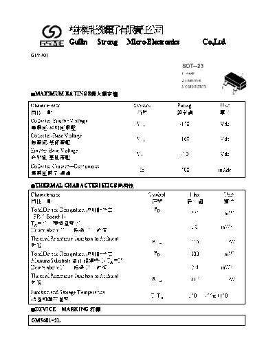
DEVICE MARKING
GM5401=2L
Guilin Strong Micro-Electronics Co.,Ltd.
GM5401
ELECTRICAL CHARACTERISTICS
(TA=25
25 unless otherwise noted 25)
Characteristic Symbol Min Max Unit
Collector-Emitter Breakdown Voltage(3)
V(BR)CEO -150 -- Vdc
-(Ic=-1.0mAdc,IB=0)
Collector-Base Breakdown Voltage
V(BR)CBO -160 -- Vdc
-(Ic=-100Adc,IE=0)
Emitter-Base Breakdown Voltage
V(BR)EBO -5.0 -- Vdc
(IE=-10Adc,Ic=0)
Emitter Cutoff Current
(VEB=-3.0Vdc,Ic=0) IEBO -- -50 nAdc
Collector Cutoff Current
ICBO -- -50 nAdc
(VCB=-120Vdc,IE=0)
DC Current Gain HFE --
(Ic=-1.0mAdc,VCE=-5.0Vdc) 50 --
(Ic=-10mAdc,VCE=-5.0Vdc) 60 240
(Ic=-50mAdc,VCE=-5.0Vdc) 30 --
Collector-Emitter Saturation Voltage
-
VCE(sat) Vdc
(Ic=-10mAdc, IB=-1.0mAdc) -- -0.2
(Ic=-50mAdc, IB=-10mAdc) -- -0.5
Base-Emitter Saturation Voltage
-
(Ic=-10mAdc, IB=-1.0mAdc) VBE(sat) -- -1.0 Vdc
(Ic=-50mAdc, IB=-5.0mAdc) -- -1.0
Current-Gain-Bandwidth Product -
(Ic=-10mAdc,VCE=-10Vdc,f=100MHz) fT 100 300 MHz
Output Capacitance
(VCB=-10.0Vdc, IE=0, f=1.0MHz) Cobo -- 6.0 pF
Small-Signal Current Gain
hfe 40 200 --
(VCE=-10Vdc, IC=-1.0mAdc, f=1.0KHz)
Noise Figure
NF -- 8.0 dB
(VCE=-5.0Vdc, IC=-200Adc,Rs=1.0kf=1.0KHz)
FR-5=1.0◦ Jabse Service Manual Search 2026 ◦ Jabse Pravopis ◦ onTap.bg ◦ Other service manual resources online : Fixya ◦ eServiceinfo