Service Manuals, User Guides, Schematic Diagrams or docs for : . Electronic Components Datasheets Active components Transistors Fairchild Semiconductor fdc6301n
<< Back | HomeMost service manuals and schematics are PDF files, so You will need Adobre Acrobat Reader to view : Acrobat Download Some of the files are DjVu format. Readers and resources available here : DjVu Resources
For the compressed files, most common are zip and rar. Please, extract files with Your favorite compression software ( WinZip, WinRAR ... ) before viewing. If a document has multiple parts, You should download all, before extracting.
Good luck. Repair on Your own risk. Make sure You know what You are doing.
Image preview - the first page of the document
>> Download fdc6301n documenatation <<
Text preview - extract from the document
September 2001
FDC6301N
Dual N-Channel , Digital FET
General Description Features
These dual N-Channel logic level enhancement mode field 25 V, 0.22 A continuous, 0.5 A Peak.
effect transistors are produced using Fairchild 's proprietary, RDS(ON) = 5 @ VGS= 2.7 V
high cell density, DMOS technology. This very high density RDS(ON) = 4 @ VGS= 4.5 V.
process is especially tailored to minimize on-state resistance.
This device has been designed especially for low voltage Very low level gate drive requirements allowing direct
applications as a replacement for digital transistors. Since bias operation in 3V circuits. VGS(th) < 1.5V.
resistors are not required, these N-Channel FET's can replace
Gate-Source Zener for ESD ruggedness.
several digital transistors, with a variety of bias resistors.
>6kV Human Body Model.
TM TM
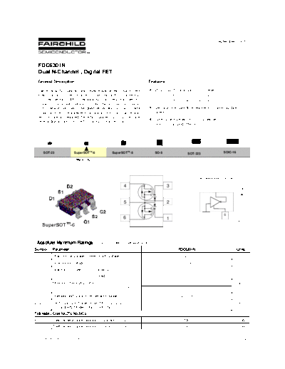
SOT-23 SuperSOT -6 SuperSOT -8 SO-8 SOT-223 SOIC-16
Mark: .301
INVERTER APPLICATION Vcc
4 3 D
OUT
5 2
IN G S
6 1
GND
Absolute Maximum Ratings TA = 25oC unless other wise noted
Symbol Parameter FDC6301N Units
VDSS, VCC Drain-Source Voltage, Power Supply Voltage 25 V
VGSS, VIN Gate-Source Voltage, VIN - 0.5 to +8 V
ID, IOUT Drain/Output Current - Continuous 0.22 A
- Pulsed 0.5
PD Maximum Power Dissipation (Note 1a) 0.9 W
(Note 1b)
0.7
TJ,TSTG Operating and Storage Temperature Range -55 to 150 ◦ Jabse Service Manual Search 2026 ◦ Jabse Pravopis ◦ onTap.bg ◦ Other service manual resources online : Fixya ◦ eServiceinfo