Service Manuals, User Guides, Schematic Diagrams or docs for : . Electronic Components Datasheets Active components Transistors KEC ktk5131s

<< Back | Home

Most service manuals and schematics are PDF files, so You will need Adobre Acrobat Reader to view : Acrobat Download Some of the files are DjVu format. Readers and resources available here : DjVu Resources
For the compressed files, most common are zip and rar. Please, extract files with Your favorite compression software ( WinZip, WinRAR ... ) before viewing. If a document has multiple parts, You should download all, before extracting.
Good luck. Repair on Your own risk. Make sure You know what You are doing.


Image preview - the first page of the document
ktk5131s


>> Download ktk5131s documenatation <<

Text preview - extract from the document
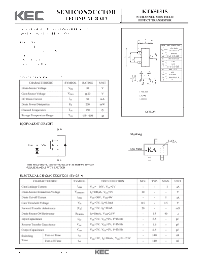
                                   SEMICONDUCTOR                                                                       KTK5131S
                                                                                                                  N CHANNEL MOS FIELD
                                             TECHNICAL DATA                                                        EFFECT TRANSISTOR


  ULTRA-HIGH SPEED SWITCHING APPLICATIONS
  ANALOG SWITCH APPLICATIONS
                                                                                                                               E
  FEATURES                                                                                                         L           B           L
                                                                                                                                                      DIM       MILLIMETERS
    2.5 Gate Drive.                                                                                                                                    A               _
                                                                                                                                                                  2.93 + 0.20
    Low Threshold Voltage : Vth=0.5           1.5V.                                                                                                   B         1.30+0.20/-0.15
                                                                                                                                                      C            1.30 MAX


                                                                                                                                                 D
                                                                                                                   2
    High Speed.                                                                                                                            3          D         0.45+0.15/-0.05


                                                                                                  A

                                                                                                      G
                                                                                                                                                      E         2.40+0.30/-0.20
    Small Package.


                                                                                                              H
                                                                                                                   1
                                                                                                                                                      G              1.90
    Enhancement-Mode.                                                                                                                                 H              0.95
                                                                                                                                                      J         0.13+0.10/-0.05
                                                                                                                                                       K            0.00 ~ 0.10
                                                                                                                       P               P               L            0.55
                                                                                                                                                      M           0.20 MIN
  MAXIMUM RATING (Ta=25                  )                                                                                                            N         1.00+0.20/-0.10


                                                                                                              N
                                                                                                          C


                                                                                                                                                J
                                                                                                                                                      P              7
           CHARACTERISTIC                    SYMBOL            RATING           UNIT                                               M


                                                                                                                       K
    Drain-Source Voltage                      VDS                  30            V
                                                                                                                   1. SOURCE
    Gate-Source Voltage                       VGSS                  20           V
                                                                                                                   2. GATE

    DC Drain Current                           ID                  50           mA                                 3. DRAIN


    Drain Power Dissipation                    PD                  200          mW
    Channel Temperature                        Tch                 150
                                                                                                                               SOT-23
    Storage Temperature Range                 Tstg             -55 150

  EQUIVALENT CIRCUIT
                                     D

                                                                                                          Marking

                                                                                                                                                                    Lot No.
           G
                                                                                                      Type Name
                                                                                                                                   KA
                                     S

        THIS TRANSISTOR IS ELECTROSTATIC SENSITIVE DEVICE.
        PLEASE HANDLE WITH CAUTION.


  ELECTRICAL CHARACTERISTICS (Ta=25                            )
                CHARACTERISTIC                       SYMBOL                      TEST CONDITION                    MIN.                        TYP.   MAX.                 UNIT
    Gate Leakage Current                               IGSS              VGS=   16V, VDS=0V                                -                    -               1                 A
    Drain-Source Breakdown Voltage                   V(BR)DSS            ID=100 A, VGS=0V                              30                       -           -                 V
    Drain Cut-off Current                              IDSS              VDS=30V, VGS=0V                                   -                    -           1                     A
    Gate Threshold Voltage                              Vth              VDS=3V, ID=0.1mA                              0.5                      -          1.5                V
    Forward Transfer Admittance                        |Yfs|             VDS=3V, ID=10mA                               20                       -           -                mS
    Drain-Source ON Resistance                        RDS(ON)            ID=10mA, VGS=2.5V                                 -                    15         40
    Input Capacitance                                  Ciss              VDS=3V, VGS=0V, f=1MHz                            -                   5.5          -                 pF
    Reverse Transfer Capacitance                       Crss              VDS=3V, VGS=0V, f=1MHz                            -                   1.6          -                 pF
    Output Capacitance                                 Coss              VDS=3V, VGS=0V, f=1MHz                            -                   6.5          -                 pF

    Switching            Turn-on Time                   ton                                                                -                   140          -                 nS
                                                                         VDD=3V, ID=10mA, VGS=0   2.5V
    Time                 Turn-off Time                  toff                                                               -                   140          -                 nS


2001. 10. 23                     Revision No : 0                                                                                                                                      1/3
                                 KTK5131S


2001. 10. 23   Revision No : 0              2/3
                                 KTK5131S


2001. 10. 23   Revision No : 0              3/3


◦ Jabse Service Manual Search 2024 ◦ Jabse PravopisonTap.bg ◦ Other service manual resources online : FixyaeServiceinfo