Service Manuals, User Guides, Schematic Diagrams or docs for : . Electronic Components Datasheets Active components Transistors KEC kgt15n120ndh
<< Back | HomeMost service manuals and schematics are PDF files, so You will need Adobre Acrobat Reader to view : Acrobat Download Some of the files are DjVu format. Readers and resources available here : DjVu Resources
For the compressed files, most common are zip and rar. Please, extract files with Your favorite compression software ( WinZip, WinRAR ... ) before viewing. If a document has multiple parts, You should download all, before extracting.
Good luck. Repair on Your own risk. Make sure You know what You are doing.
Image preview - the first page of the document
>> Download kgt15n120ndh documenatation <<
Text preview - extract from the document
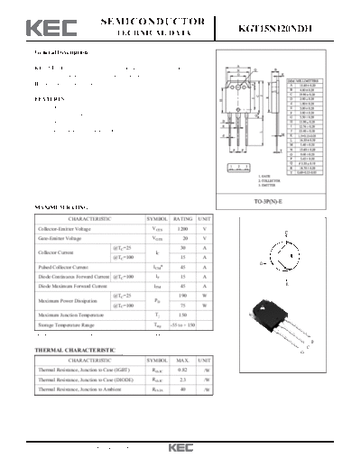
SEMICONDUCTOR
TECHNICAL DATA
KGT15N120NDH
General Description
KEC NPT IGBTs offer low switching losses, high energy efficiency
and high avalanche ruggedness for soft switching application such as
IH(induction heating), microwave oven, etc.
FEATURES
High speed switching
High system efficiency
Soft current turn-off waveforms
Extremely enhanced avalanche capability
MAXIMUM RATING (Ta=25 )
CHARACTERISTIC SYMBOL RATING UNIT
Collector-Emitter Voltage VCES 1200 V
Gate-Emitter Voltage VGES 20 V
@TC=25 30 A
Collector Current IC
@TC=100 15 A
Pulsed Collector Current ICM* 45 A
Diode Continuous Forward Current @TC=100 IF 15 A
Diode Maximum Forward Current IFM 45 A
@TC=25 190 W
Maximum Power Dissipation PD
@TC=100 75 W
Maximum Junction Temperature Tj 150
Storage Temperature Range Tstg -55 to + 150
*Repetitive rating : Pulse width limited by max. junction temperature
E
C
THERMAL CHARACTERISTIC G
CHARACTERISTIC SYMBOL MAX. UNIT
Thermal Resistance, Junction to Case (IGBT) Rt h JC 0.82 /W
Thermal Resistance, Junction to Case (DIODE) Rt h JC 2.3 /W
Thermal Resistance, Junction to Ambient Rt h JA 40 /W
2011. 8. 11 Revision No : 0 1/7
KGT15N120NDH
ELECTRICAL CHARACTERISTICS (Ta=25 )
CHARACTERISTIC SYMBOL TEST CONDITION MIN. TYP. MAX. UNIT
Static
Collector-Emitter Breakdown Voltage BVCES VGE=0V , IC=1.0mA 1200 - - V
Collector Cut-off Current ICES VGE=0V, VCE=1200V - - 1.0 mA
Gate Leakage Current IGES VCE=0V, VGE= 20V - - 100 nA
Gate Threshold Voltage VGE(th) VGE=VCE, IC=15mA 4.5 6.0 7.5 V
VGE=15V, IC=15A - 1.85 2.25 V
Collector-Emitter Saturation Voltage VCE(sat) VGE=15V, IC=15A, TC = 125 - 2.15 - V
VGE=15V, IC=30A - 2.40 - V
Dynamic
Total Gate Charge Qg - 90 150 nC
Gate-Emitter Charge Qge VCC=600V, VGE=15V, IC= 15A - 15 - nC
Gate-Collector Charge Qgc - 40 - nC
Turn-On Delay Time td(on) - 30 - ns
Rise Time tr - 30 - ns
Turn-Off Delay Time td(off) - 150 - ns
VCC=600V, IC=15A, VGE=15V,RG=10
Fall Time tf - 150 220 ns
Inductive Load, TC = 25
Turn-On Switching Loss Eon - 2.1 - mJ
Turn-Off Switching Loss Eoff - 0.8 - mJ
Total Switching Loss Ets - 3.0 - mJ
Turn-On Delay Time td(on) - 35 - ns
Rise Time tr - 35 - ns
Turn-Off Delay Time td(off) - 180 - ns
VCC=600V, IC=15A, VGE=15V, RG=10
Fall Time tf - 250 - ns
Inductive Load, TC = 125
Turn-On Switching Loss Eon - 2.5 - mJ
Turn-Off Switching Loss Eoff - 1.7 - mJ
Total Switching Loss Ets - 4.5 - mJ
Input Capacitance Cies - 1600 - pF
Ouput Capacitance Coes VCE=30V, VGE=0V, f=1MHz - 60 - pF
Reverse Transfer Capacitance Cres - 40 - pF
Marking
2011. 8. 11 Revision No : 0 2/7
KGT15N120NDH
ELECTRICAL CHARACTERISTIC OF DIODE
CHARACTERISTIC SYMBOL TEST CONDITION MIN. TYP. MAX. UNIT
TC=25 - 1.8 2.5
Diode Forward Voltage VF IF = 15A V
TC=125 - 1.9 -
TC=25 - 230 300
Diode Reverse Recovery Time trr ns
TC=125 - 270 -
IF = 15A TC=25 - 24 31
Diode Peak Reverse Recovery Current Irr A
di/dt = 200A/ s TC=125 - 27 -
TC=25 - 2400 4000
Diode Reverse Recovery Charge Qrr nC
TC=125 - 3640 -
2011. 8. 11 Revision No : 0 3/7
KGT15N120NDH
2011. 8. 11 Revision No : 0 4/7
KGT15N120NDH
2011. 8. 11 Revision No : 0 5/7
KGT15N120NDH
2011. 8. 11 Revision No : 0 6/7
KGT15N120NDH
2011. 8. 11 Revision No : 0 7/7
◦ Jabse Service Manual Search 2026 ◦ Jabse Pravopis ◦ onTap.bg ◦ Other service manual resources online : Fixya ◦ eServiceinfo