Service Manuals, User Guides, Schematic Diagrams or docs for : . Electronic Components Datasheets Active components Transistors KEC kmc7d0cn20ca
<< Back | HomeMost service manuals and schematics are PDF files, so You will need Adobre Acrobat Reader to view : Acrobat Download Some of the files are DjVu format. Readers and resources available here : DjVu Resources
For the compressed files, most common are zip and rar. Please, extract files with Your favorite compression software ( WinZip, WinRAR ... ) before viewing. If a document has multiple parts, You should download all, before extracting.
Good luck. Repair on Your own risk. Make sure You know what You are doing.
Image preview - the first page of the document
>> Download kmc7d0cn20ca documenatation <<
Text preview - extract from the document
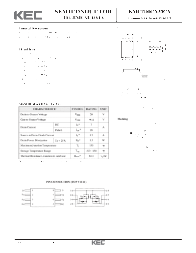
                                    SEMICONDUCTOR                                                     KMC7D0CN20CA
                                             TECHNICAL DATA                                          Common N-Ch Trench MOSFET


  General Description
  Switching regulator and DC-DC Converter applications.                                               C

  It's mainly suitable for Li-ion battery pack.
                                                                                                                                 D
                                                                                                8         5

                                                                                                                                                 A
  FEATURES                                                                                                     E1   E
                                                                                                                             B
                                                                                                                                            A1
    VDSS=20V, ID=7A.
                                                                                                1         4
    Low Drain to Source On Resistance.
     : RDS(ON)=20.5m (Max.) @ VGS=4.5V
                                                                                                                                 DIM      MILLIMETERS
     : RDS(ON)=21.0m (Max.) @ VGS=4.0V                                                                                            A         1.2 MAX
                                                                                                                                  A1        0.15 MAX
     : RDS(ON)=22.5m (Max.) @ VGS=3.1V
                                                                                                                                     B            _
                                                                                                                                             0.28 + 1
     : RDS(ON)=26.0m (Max.) @ VGS=2.5V                                                                              GAUGE            C     0.65 Typ.
                                                                                                                    PLANE                      _
                                                                                                                                           3.0 + 0.10
                                                                                                                                     D
    ESD Protection.                                                                                                                  E          _
                                                                                                                                           6.40 + 0.20
                                                                                                                                     E1          _
                                                                                                                                            4.40 + 0.10
    Super High Dense Cell Design.                                                                                                                _
                                                                                                                                     L      0.50 + 0.20


                                                                                              0.25
                                                                                                                    L


  MAXIMUM RATING (Ta=25                  )
                   CHARACTERISTIC                     SYMBOL        RATING       UNIT                               TSSOP-8

   Drain to Source Voltage                             VDSS           20          V
   Gate to Source Voltage                              VGSS            12         V         Marking

                                    DC                  ID *           7                                                    Type Name
   Drain Current                                                                  A
                                    Pulsed              IDP *         28
   Source to Drain Diode Current                        IS *          1.7         A                           KMC7D0
                                                                                                              CN20CA
   Drain Power Dissipation          Ta = 25             PD *          1.5         W
   Maximum Junction Temperature                          Tj           150
   Storage Temperature Range                            Tstg        -55 150                                                  Lot No.
   Thermal Resistance, Junction to Ambient             RthJA*        83.3         /W
  Note > *Surface Mounted on 1" 1" FR4 Board, t
◦ Jabse Service Manual Search 2026 ◦ Jabse Pravopis ◦ onTap.bg ◦ Other service manual resources online : Fixya ◦ eServiceinfo