Service Manuals, User Guides, Schematic Diagrams or docs for : . Electronic Components Datasheets Active components Transistors KEC kml0d4n20v
<< Back | HomeMost service manuals and schematics are PDF files, so You will need Adobre Acrobat Reader to view : Acrobat Download Some of the files are DjVu format. Readers and resources available here : DjVu Resources
For the compressed files, most common are zip and rar. Please, extract files with Your favorite compression software ( WinZip, WinRAR ... ) before viewing. If a document has multiple parts, You should download all, before extracting.
Good luck. Repair on Your own risk. Make sure You know what You are doing.
Image preview - the first page of the document
>> Download kml0d4n20v documenatation <<
Text preview - extract from the document
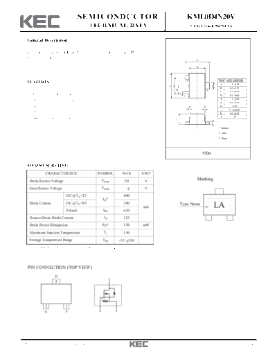
SEMICONDUCTOR KML0D4N20V
TECHNICAL DATA N-Ch Trench MOSFET
General Description
It's mainly suitable for Load Switching Cell Phones, Battery Powered
Systems and Level-Shifter. E
B
2 DIM MILLIMETERS
FEATURES A _
1.2 +0.05
D
G
A
_
VDSS=20V, ID=0.4A B 0.8 +0.05
H
1 3 _
C 0.5 + 0.05
Drain-Soure ON Resistance
K
D _
0.3 + 0.05
E _
1.2 + 0.05
: RDS(ON)=0.70 @ VGS=4.5V G _
0.8 + 0.05
: RDS(ON)=0.85 @ VGS=2.5V P P H 0.40
J _
0.12 + 0.05
: RDS(ON)=1.25 @ VGS=1.8V K _
0.2 + 0.05
P 5
Super High Dense Cell Design
C
J
1. Source
2. Gate
3. Drain
VSM
MAXIMUM RATING (Ta=25 )
CHARACTERISTIC SYMBOL N-Ch UNIT
Drain-Source Voltage VDSS 20 V Marking
Gate-Source Voltage VGSS 6 V
DC @TA=25 400
ID*
Drain Current DC @TA=85 280
Pulsed IDP 650
mA
Type Name
LA
Source-Drain Diode Current IS 125
Drain Power Dissipation P D* 150 mW
Maximum Junction Temperature Tj 150
Storage Temperature Range Tstg -55 150
Note 1) *Surface Mounted on 1" 1" FR4 Board. t 5 sec
PIN CONNECTION (TOP VIEW)
D
3 3
2 1
G S 2 1
2012. 3. 5 Revision No : 0 1/4
KML0D4N20V
ELECTRICAL CHARACTERISTICS (Ta=25 )
CHARACTERISTIC SYMBOL TEST CONDITION MIN. TYP. MAX. UNIT
Static
Drain-Source Breakdown Voltage BVDSS ID=250 A, VGS=0V 20 - - V
Drain Cut-off Current IDSS VGS=0V, VDS=16V - 0.3 100 nA
Gate Leakage Current IGSS VGS= 4.5V, VDS=0V - 0.5 1.0 A
Gate Threshold Voltage Vth VDS=VGS, ID=250 A 0.45 - 1.0 V
VGS=4.5V, ID=400mA - 0.41 0.70
Drain-Source ON Resistance RDS(ON)* VGS=2.5V, ID=350mA - 0.53 0.85
VGS=1.8V, ID=300mA - 0.70 1.25
Forward Transconductance gfs* VDS=10V, ID=400mA - 1.0 - S
Source-Drain Diode Forward Voltage VSD* IS=150mA, VGS=0V - 0.8 1.2 V
Dynamic
Total Gate Charge Qg* - 750 -
Gate-Source Charge Qgs* VDS=10V, ID=250mA, VGS=4.5V - 75 - pC
Gate-Drain Charge Qgd* - 225 -
Turn-on Delay time td(on)* - 5 -
VDD=10V, ID=200mA,
ns
VGS=4.5V, RG=10
Turn-off Delay time td(off)* - 25 -
Note 2) *Pulse test : Pulse width 300 , Duty Cycle 2%.
2012. 3. 5 Revision No : 0 2/4
KML0D4N20V
Fig 1. ID - VDS Fig 2. RDS(on) - ID
Drain-Source On Resistance RDS(on) ()
1.0 4.0
VGS=2.5V
VGS=1.8V
0.8 3.2
Drain Current ID (A)
VGS=2.0V
0.6 2.4
VGS=5,4,3V
0.4 1.6
VGS=2.5V VGS=1.8V
0.2 0.8
VGS=1.0V
VGS=4.5V
0.0 0.0
0.0 0.5 1.0 1.5 2.0 2.5 3.0 0 0.2 0.4 0.6 0.8 1.0
Drain - Source Voltage VDS (V) Drain - Current ID (A)
Fig 3. ID - VGS Fig 4. RDS(ON) - Tj
Normalized Drain-Source On Resistance RDS(on) ()
1.0 1.6
VGS = 4.5V
-55 C ID = 350mA
0.8 1.4
Drain Current ID (A)
TC=125 C
25 C
0.6 1.2
0.4 1.0
0.2 0.8
0.0 0.6
0.0 0.5 1.0 1.5 2.0 2.5 -50 -25 0 25 50 75 100 125
Gate - Source Voltage VGS (V) Junction Temperature Tj ( C)
Fig 5. Vth - Tj Fig 6. IDR - VSDF
0.3 1000
Reverse Drain Current IDR (mA)
Gate Threshold Voltage Vth (V)
ID = 250◦ Jabse Service Manual Search 2026 ◦ Jabse Pravopis ◦ onTap.bg ◦ Other service manual resources online : Fixya ◦ eServiceinfo