Service Manuals, User Guides, Schematic Diagrams or docs for : . Electronic Components Datasheets Active components Transistors KEC krc828f

<< Back | Home

Most service manuals and schematics are PDF files, so You will need Adobre Acrobat Reader to view : Acrobat Download Some of the files are DjVu format. Readers and resources available here : DjVu Resources
For the compressed files, most common are zip and rar. Please, extract files with Your favorite compression software ( WinZip, WinRAR ... ) before viewing. If a document has multiple parts, You should download all, before extracting.
Good luck. Repair on Your own risk. Make sure You know what You are doing.


Image preview - the first page of the document
krc828f


>> Download krc828f documenatation <<

Text preview - extract from the document
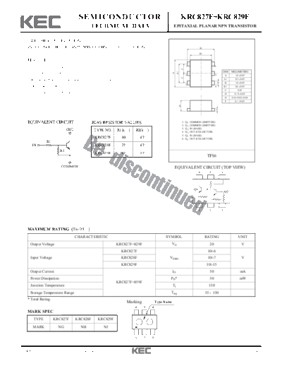
                                    SEMICONDUCTOR                                                         KRC827F~KRC829F
                                            TECHNICAL DATA                                      EPITAXIAL PLANAR NPN TRANSISTOR


  SWITCHING APPLICATION.
  INTERFACE CIRCUIT AND DRIVER CIRCUIT APPLICATION.                                                                                B

                                                                                                                               B1

  FEATURES
                                                                                                                   1                           6
    With Built-in Bias Resistors.


                                                                                                              C
                                                                                                                                                           DIM   MILLIMETERS


                                                                                                     A1
                                                                                                A
    Simplify Circuit Design.                                                                                       2                           5            A           _
                                                                                                                                                                    1.0 + 0.05


                                                                                                              C
                                                                                                                                                            A1          _
                                                                                                                                                                    0.7 + 0.05
    Reduce a Quantity of Parts and Manufacturing Process.
                                                                                                                                                                        _


                                                                                                                                                   D
                                                                                                                                                            B       1.0 + 0.05
                                                                                                                   3
    High Packing Density.                                                                                                                      4            B1          _
                                                                                                                                                                    0.8 + 0.05
                                                                                                                                                            C          0.35
    Thin Fine Pitch Super mini 6 pin Package.                                                                                                               D            _
                                                                                                                                                                    0.15 + 0.05
                                                                                                                                                            H    0.38+0.02/-0.04
                                                                                                                                                            T           _
                                                                                                                                                                    0.1 + 0.05


                                                                                                          H


                                                                                                                                                   T
  EQUIVALENT CIRCUIT                         BIAS RESISTOR VALUES                                             1.   Q1   COMMON (EMITTER)
                                                                                                              2.   Q2   COMMON (EMITTER)
                                                                                                              3.   Q2   IN (BASE)
                             OUT              TYPE NO.    R1(k


◦ Jabse Service Manual Search 2024 ◦ Jabse PravopisonTap.bg ◦ Other service manual resources online : FixyaeServiceinfo