Service Manuals, User Guides, Schematic Diagrams or docs for : . Electronic Components Datasheets Active components Transistors HT Semiconductor umf21n

<< Back | Home

Most service manuals and schematics are PDF files, so You will need Adobre Acrobat Reader to view : Acrobat Download Some of the files are DjVu format. Readers and resources available here : DjVu Resources
For the compressed files, most common are zip and rar. Please, extract files with Your favorite compression software ( WinZip, WinRAR ... ) before viewing. If a document has multiple parts, You should download all, before extracting.
Good luck. Repair on Your own risk. Make sure You know what You are doing.


Image preview - the first page of the document
umf21n


>> Download umf21n documenatation <<

Text preview - extract from the document
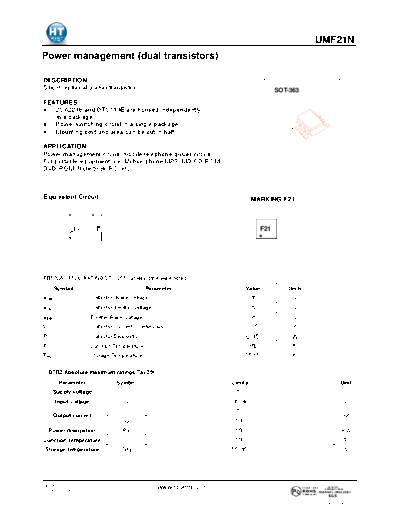
                                                                                                                UMF21N
Power management (dual transistors)

DESCRIPTION
Silicon epitaxial planar transistor                                                                  SOT-363
FEATURES
   2SA2018 and DTC114E are housed independently
   in a package.
   Power switching circuit in a single package.
   Mounting cost and area can be cut in half.                                                            1


APPLICATION
Power management circuit, mobile telephone quiver circuit
For portable equipment:(i.e. Mobile phone,MP3, MD,CD-ROM,
DVD-ROM, Note book PC, etc.)


Equivalent Circuit                                                                       MARKING:F21
            (3)                   (2)   (1)


         DTr2
                       R1
                                          Tr1                                                  F21
                  R2

            (4)             (5)         (6)


TR1 MAXIMUM RATINGS Ta=25 unless otherwise noted
       Symbol                                             Parameter                   Value             Units
VCBO                          Collector- Base Voltage                                   -15               V
VCEO                          Collector-Emitter Voltage                                 -12               V
VEBO                          Emitter-Base Voltage                                       -6               V
IC                            Collector Current -Continuous                             -0.5              A
PC                            Collector Dissipation                                    0.15              W
TJ                            Junction Temperature                                      150               
Tstg                          Storage Temperature                                     -55-150             


     DTR2 Absolute maximum ratings(Ta=25)
         Parameter                              Symbol                         Limits                                     Unit
       Supply voltage                            VCC                             50                                         V
       Input voltage                             VIN                           -10~40                                       V
                                                  IO                             50
       Output current                                                                                                      mA
                                                IC(MAX)                         100
     Power dissipation                           Pd                             150                                        mW
Junction temperature                              Tj                            150                                         
 Storage temperature                             Tstg                          -55~150                                      


1
JinYu                                                         www.htsemi.com
semiconductor

                                                                                                                Date:2011/ 05
                                                                                                                 EMF23


 TR1 ELECTRICAL CHARACTERISTICS (Ta=25 unless otherwise specified)

            Parameter                         Symbol           Test      conditions          Min       Typ       Max     Unit

Collector-base breakdown voltage              V(BR)CBO   IC=-10A, IE=0                       -15                             V

Collector-emitter breakdown voltage           V(BR)CEO   IC=-1mA, IB=0                       -12                             V

Emitter-base breakdown voltage                V(BR)EBO   IE=-10A, IC=0                        -6                             V

Collector cut-off current                       ICBO     VCB= -15 V, IE=0                                       -0.1     A
Emitter cut-off current                         IEBO     VEB=- 6V, IC=0                                         -0.1     A
DC current gain                                 hFE      VCE=-2V, IC=-10mA                   270                680

Collector-emitter saturation voltage          VCE(sat)   IC=-200mA,IB=-10mA                                     -0.25        V

Transition frequency                             fT      VCE=-2V,IC=-10mA, f=100MHz                   260               MHz

Collector output capacitance                    Cob      VCB=-10V,IE=0,f=1MHz                          6.5               pF


DTR2     Electrical characteristics (Ta=25)
      Parameter               Symbol     Min.            Typ          Max.            Unit             Conditions

                            VI(off)                                   0.5                          VCC=5V ,IO=100A
      Input voltage                                                                   V
                            VI(on)        3                                                        VO=0.3V ,IO=10 mA

    Output voltage          VO(on)                                    0.3             V            IO/II=10mA/0.5mA

     Input current             II                                     0.88            mA                VI=5V

    Output current           IO(off)                                  0.5             A              VCC=50V, VI=0

    DC current gain            GI         30                                                        VO=5V ,IO=5mA

    Input resistance           R1         7              10           13              K

    Resistance ratio        R2/R1        0.8             1            1.2

Transition frequency           fT                        250                      MHz         VCE=10V ,IE=-5mA,f=100MHz


2
JinYu                                          www.htsemi.com
semiconductor

                                                                                                             Date:2011/ 05


◦ Jabse Service Manual Search 2024 ◦ Jabse PravopisonTap.bg ◦ Other service manual resources online : FixyaeServiceinfo