Service Manuals, User Guides, Schematic Diagrams or docs for : . Electronic Components Datasheets Active components Transistors Isahaya 2sc5626
<< Back | HomeMost service manuals and schematics are PDF files, so You will need Adobre Acrobat Reader to view : Acrobat Download Some of the files are DjVu format. Readers and resources available here : DjVu Resources
For the compressed files, most common are zip and rar. Please, extract files with Your favorite compression software ( WinZip, WinRAR ... ) before viewing. If a document has multiple parts, You should download all, before extracting.
Good luck. Repair on Your own risk. Make sure You know what You are doing.
Image preview - the first page of the document
>> Download 2sc5626 documenatation <<
Text preview - extract from the document
Transistor
2SC5626
For High Frequency Amplify Application
Silicon NPN Epitaxial Type (Super Mini type)
DESCURIPTION
Mitsubishi 2SC5626 is a super mini packege resin sealed
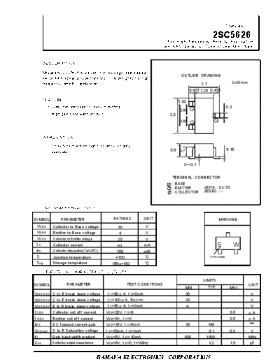
OUTLINE DRAWING
silicon NPN epitaxial ty pe transistor. It is designed f or high
f requency amplif y application. 2.1 Unit:mm
0.425 1.25 0.425
FEATURE 1.30
Super mini package f or easy mounting 0.3
0.65 1
High gain band width product 2.0
0.65 2
3
APPLICATION
Small ty pe machine high f requency amplif y
0.9 0.7 0.15
application
00.1
TERMINAL CONNECTOR
1 : BASE
2 : EMITTER JEITA : SC-70
3 : COLLECTOR JEDEC : -
MAXIMUM RATINGS (Ta=25)
SY MBOL PARAMETER RATINGS UNIT MARKING
VCBO Collector to Base v oltage 30 V
VEBO Emitter to Base v oltage 4 V
VCEO Collector to Emitter voltage 20 V
I C Collector current 50 mA S W
PC Collector dissipation(Ta=25) 150 mW
Tj Junction temperature +150 TYPE NAME
Tstg Storage temprature -55to+150
ELECTRICAL CHARACTERISTICS (Ta=25)
LIMITS
SY MBOL PARAMETER TEST CONDITIONS UNIT
MIN TY P MAX
V(BR)CBO C to B break down v oltage I C=50 A, I E =0mA 30 V
V(BR)CEO C to E break down v oltage I C=100 A, R BE = 20 V
V(BR)EBO E to B break down v oltage I C=50 A, I C=0mA 4 V
I CBO Collector cut cf f current VCB =20V, I E =0 0.5 A
I EBO Emitter cut of f current VEB =3V, I C=0 0.5 A
hFE DC f orward current gain VCE =10V, I C=5mA 50 148
VCE(sat) C to E Saturation v oltage I C=10mA, I B =1mA 0.1 0.3 V
fT Gain band width product VCE =5V, I E =-10mA 600 1100 MHz
C ob Collector output capacitance VCB =6V, I E =0, f =1MHz 1.2 1.5 pF
ISAHAYA ELECTRONICSCORPORATION
Transistor
2SC5626
For High Frequency Amplify Application
Silicon NPN Epitaxial Type (SuperMini type)
C o m m o t p u t
n emitter ou Common emitter transfer
20
180 A 160 A Ta=25
100
18
V CE=6V 140 A
Ta=25 16
120 A
14 100 A
10
12 80 A
10
60 A
8
1 6
40 A
4 20 A
2
IB=0 A
0
0.1
0 2 4 6 8 10 12 14 16 18 20
0 0.2 0.4 0.6 0.8 1 1.2 1.4 1.6
collector to emitter voltage ) V CE(V)
VCE(V
base to collector voltage VBE (V)
V BE(V)
DC forward current gain collector to emitter voltage
t
VS. collector curren V S . c o lr r e n t
lector cu
10000 10
Ta=25
Ta=25
IC/IB=10/1
VCE=10V
1000
1
100
0.1
10
0.01
1
0.1 110 100 1000 0.11 10 100
collector current
I IC (mA)
C(mA)
collector I IC(mA)
current C (mA)
Gain band width product collector output/input capacitance
V S . C o l t a g e
lector to Base Vol
VS. Emitter current
10000 100.0
V CE=5V f=1MHz
Ta=25 IE=0A
IC=0A
Ta=25
1000 10.0
Cob
100 1.0
Cib
10 0.1
0.1 1 10100 0.11.010.0 100.0
V
collector to base voltage VC BCB(V)
(V)
emitter IE (mA)
current I E (mA) emitter to base voltage VE BEB(V)
V (V)
ISAHAYA ELECTRONICSCORPORATION
Transistor
2SC5626
For High Frequency Amplify Application
Silicon NPN Epitaxial Type (SuperMini type)
C o l l e c t o t i m e c o n s t a n t
r to base
VS. Emitter current
100
VCB=5V
f=31.8MHz
Ta=25
10
1
0.1 1.0 10.0
emitter I IEE(mA)
current (mA)
ISAHAYA ELECTRONICSCORPORATION
Marketing division, Marketing planning department
6-41 Tsukuba, Isahaya, Nagasaki, 854-0065 Japan
Keep safety first in your circuit designs!
◦ Jabse Service Manual Search 2026 ◦ Jabse Pravopis ◦ onTap.bg ◦ Other service manual resources online : Fixya ◦ eServiceinfo