Service Manuals, User Guides, Schematic Diagrams or docs for : . Electronic Components Datasheets Active components Transistors LGE mmbt3904

<< Back | Home

Most service manuals and schematics are PDF files, so You will need Adobre Acrobat Reader to view : Acrobat Download Some of the files are DjVu format. Readers and resources available here : DjVu Resources
For the compressed files, most common are zip and rar. Please, extract files with Your favorite compression software ( WinZip, WinRAR ... ) before viewing. If a document has multiple parts, You should download all, before extracting.
Good luck. Repair on Your own risk. Make sure You know what You are doing.


Image preview - the first page of the document
mmbt3904


>> Download mmbt3904 documenatation <<

Text preview - extract from the document
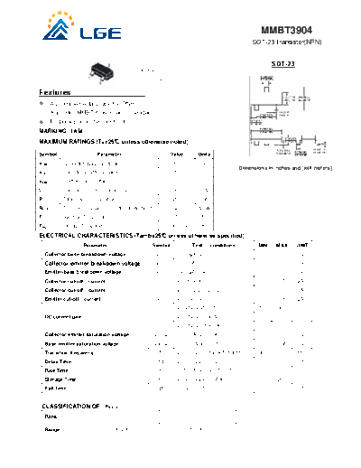
                                                                                                                 MMBT3904
                                                                                                              SOT-23 Transistor(NPN)

                                                1. BASE                                                                 SOT-23
                                                2. EMITTER
                                                3. COLLECTOR


Features
       As complementary type the PNP
       transistor MMBT3906 is recommended
       Epitaxial planar die construction
MARKING: 1AM
MAXIMUM RATINGS (TA=25 unless otherwise noted)

Symbol                        Parameter                              Value         Units
VCBO         Collector-Base Voltage                                    60               V
                                                                                                         Dimensions in inches and (millimeters)
VCEO         Collector-Emitter Voltage                                 40               V
VEBO         Emitter-Base Voltage                                      6                V
IC           Collector Current -Continuous                            200             mA
PC           Total Device Dissipation                                 200             mW
RJA          Thermal Resistance Junction to Ambient                   625          /W
TJ           Junction Temperature                                     150             
Tstg         Storage Temperature                                   -55 to +150        
ELECTRICAL CHARACTERISTICS (Tamb=25 unless otherwise specified)
                       Parameter                          Symbol                 Test       conditions          MIN       MAX      UNIT
     Collector-base breakdown voltage                        VCBO       IC= 10A, IE=0                            60                 V
     Collector-emitter breakdown voltage                     VCEO       IC= 1mA, IB=0                            40                 V
     Emitter-base breakdown voltage                          VEBO       IE=10A, IC=0                              6                 V
     Collector cut-off    current                            ICBO       VCB=60V, IE=0                                       0.1    A
     Collector cut-off    current                            ICEX       VCE=30V,VBE(off)=3V                                 50     nA
     Emitter cut-off     current                             IEBO       VEB=5V, IC=0                                        0.1    A
                                                           hFE(1)       VCE=1V, IC=10mA                          100        400
     DC current gain                                       hFE(2)       VCE=1V, IC= 50mA                         60
                                                           hFE(3)       VCE=1V, IC= 100mA                        30
     Collector-emitter saturation voltage                 VCE(sat)      IC=50mA, IB= 5mA                                    0.3     V
     Base-emitter saturation voltage                      VBE(sat)      IC= 50mA, IB= 5mA                                   0.95    V
     Transition frequency                                     fT        VCE= 20V, IC= 10mA,f=100MHz              300               MHz
     Delay Time                                               td        VCC=3V,VBE=-0.5V                                    35     nS
     Rise Time                                                tr        IC=10mA, IB1=-IB2=1.0mA                             35     nS
     Storage Time                                             ts        VCC=3.0V,IC=10mAdc                                  200    nS
     Fall Time                                                tf        IB1=-IB2=1mA                                        50     nS


 CLASSIFICATION OF                  hFE(1)
     Rank                                O                                        Y                                     G

     Range                            100-200                                200-300                                  300-400
                            MMBT3904
                          SOT-23 Transistor(NPN)

Typical Characteristics


◦ Jabse Service Manual Search 2024 ◦ Jabse PravopisonTap.bg ◦ Other service manual resources online : FixyaeServiceinfo