Service Manuals, User Guides, Schematic Diagrams or docs for : . Electronic Components Datasheets Active components Transistors LGE dtc113z
<< Back | HomeMost service manuals and schematics are PDF files, so You will need Adobre Acrobat Reader to view : Acrobat Download Some of the files are DjVu format. Readers and resources available here : DjVu Resources
For the compressed files, most common are zip and rar. Please, extract files with Your favorite compression software ( WinZip, WinRAR ... ) before viewing. If a document has multiple parts, You should download all, before extracting.
Good luck. Repair on Your own risk. Make sure You know what You are doing.
Image preview - the first page of the document
>> Download dtc113z documenatation <<
Text preview - extract from the document
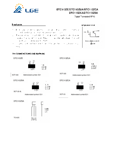
                                                         DTC113ZE/DTC113ZUA/DTC113ZCA
                                                                  DTC113ZKA/DTC113ZSA
                                                                                Digital Transistor(NPN)


Features

1.   Built-in bias resistors enable the configuration of an inverter circuit without
     connecting external input resistors(see equivalent circuit).
2.   The bias resistors consist of thin-film resistors with complete isolation to allow
     negative biasing of the input. They also have the advantage of almost
     completely eliminating parasitic effects.
3.   Only the on/off conditions need to be set for operation, making device design
     easy.


PIN CONNENCTIONS AND MARKING

 DTC113ZE                                                    DTC113ZUA


              Addreviated symbol: 24                         SOT-323
SOT-523       Addreviated symbol: E21                                         Addreviated symbol: E21


 DTC113ZKA                                                   DTC113ZCA
                                                             DTA113ZCA


   SOT-23
 SOT-23-3L
                Addreviated symbol: E21                      SOT-23         Addreviated symbol:E21


 DTC113ZSA


 TO-92S
                                                          DTC113ZE/DTC113ZUA/DTC113ZCA
                                                                   DTC113ZKA/DTC113ZSA
                                                                                    Digital Transistor(NPN)
Absolute maximum ratings(Ta=25)
                                                               Limits (DTC113Z)
      Parameter            Symbol                                                                                Unit
                                              E           UA            CA              KA            SA
    Supply voltage            VCC                                       50                                        V
     Input voltage             VIN                                    -5~+10                                      V
                                  IO                                   100
    Output current                                                                                               mA
                            IC(MAX)                                    100
  Power dissipation               Pd          150                      200                           300         mW
 Junction temperature             Tj                                   150
 Storage temperature          Tstg                                    -55~150
Electrical characteristics (Ta=25)
     Parameter            Symbol       Min.         Typ        Max.          Unit               Conditions
                           VI(off)                             0.3                           VCC=5V ,IO=100A
   Input voltage                                                               V
                           VI(on)       3                                                    VO=0.3V ,IO=20 mA
  Output voltage          VO(on)                               0.3             V             IO/II=10mA/0.5mA
   Input current             II                                7.2           mA                   VI=5V
  Output current           IO(off)                             0.5           A                 VCC=50V, VI=0
  DC current gain           GI         33                                                     VO=5V ,IO=5mA
  Input resistance          R1         0.7           1         1.3           K
  Resistance ratio        R2/R1         8           10          12
Transition frequency         fT                     250                      MHz          VCE=10V ,IE=-5mA,f=100MHz

Typical Characteristics
◦ Jabse Service Manual Search 2026 ◦ Jabse Pravopis ◦ onTap.bg ◦ Other service manual resources online : Fixya ◦ eServiceinfo