Service Manuals, User Guides, Schematic Diagrams or docs for : . Electronic Components Datasheets Active components Transistors LGE dtc114t
<< Back | HomeMost service manuals and schematics are PDF files, so You will need Adobre Acrobat Reader to view : Acrobat Download Some of the files are DjVu format. Readers and resources available here : DjVu Resources
For the compressed files, most common are zip and rar. Please, extract files with Your favorite compression software ( WinZip, WinRAR ... ) before viewing. If a document has multiple parts, You should download all, before extracting.
Good luck. Repair on Your own risk. Make sure You know what You are doing.
Image preview - the first page of the document
>> Download dtc114t documenatation <<
Text preview - extract from the document
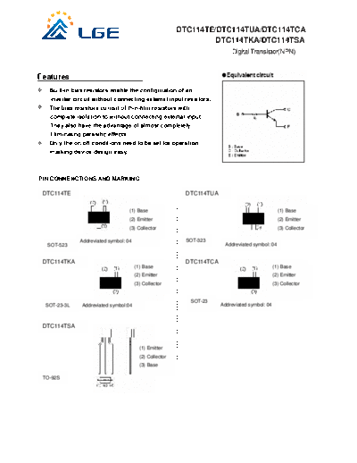
                                                         DTC114TE/DTC114TUA/DTC114TCA
                                                                  DTC114TKA/DTC114TSA
                                                                           Digital Transistor(NPN)


Features
   Built-in bias resistors enable the configuration of an
   inverter circuit without connecting extemal input resistors.
   The bias resistors conisit of thin-film resistors with
   complete isolation to without connecting extemal input.
   They also have the advantage of almost completely
   Eliminating parasitic effects.
   Only the on/off conditions need to be set for operation,
   marking device design easy.


PIN CONNENCTIONS AND MARKING

 DTC114TE                                                  DTC114TUA


                                    (1) Base                                                      (1) Base
                                                                                                    (1) Base
                                    (2) Emitter                                                   (2) Emitter
                                                                                                    (2) Emitter
                                    (3) Collector                                                 (3) Collector
                                                                                                    (3) Collector

              Addreviated symbol: 04                       SOT-323
  SOT-523                                                                Addreviated symbol: 04


 DTC114TKA                                                 DTC114TCA
                                                           DTA114ECA
                                       (1) Base                                                 (1) Base
                                                                                                  (1) Base
                                       (2) Emitter                                              (2) Emitter
                                                                                                  (2) Emitter
                                       (3) Collector                                            (3) Collector
                                                                                                  (3) Collector

                                                            SOT-23
 SOT-23-3L     Addreviated symbol:04                                   Addreviated symbol: 04


 DTC114TSA


                                         (1) Emitter
                                         (2) Collector
                                         (3) Base

 TO-92S
                                                             DTC114TE/DTC114TUA/DTC114TCA
                                                                      DTC114TKA/DTC114TSA
                                                                                         Digital Transistor(NPN)
 MAXIMUM RATINGS* TA=25 unless otherwise noted
       Symbol                      Parameter                               LIMITS(DTC114T)                           Units
                                                                E          UA      KA         CA         SA
VCBO                 Collector-Base Voltage                                        50                                 V
VCEO                 Collector-Emitter Voltage                                     50                                 V
VEBO                 Emitter-Base Voltage                                           5                                 V
IC                   Collector Current -Continuous                                 100                               mA
PC                   Collector Dissipation                     150                 200                   300         mW
Tj                   Junction temperature                                          150
TJ, Tstg             Junction and Storage Temperature                           -55~+150

 ELECTRICAL CHARACTERISTICS (Tamb=25                          unless       otherwise      specified)
           Parameter                          Symbol                Test   conditions              MIN        TYP    MAX     UNIT
 Collector-base breakdown voltage             V(BR)CBO   Ic=50
◦ Jabse Service Manual Search 2026 ◦ Jabse Pravopis ◦ onTap.bg ◦ Other service manual resources online : Fixya ◦ eServiceinfo