Service Manuals, User Guides, Schematic Diagrams or docs for : . Electronic Components Datasheets Active components Transistors LGE 2sd1899

<< Back | Home

Most service manuals and schematics are PDF files, so You will need Adobre Acrobat Reader to view : Acrobat Download Some of the files are DjVu format. Readers and resources available here : DjVu Resources
For the compressed files, most common are zip and rar. Please, extract files with Your favorite compression software ( WinZip, WinRAR ... ) before viewing. If a document has multiple parts, You should download all, before extracting.
Good luck. Repair on Your own risk. Make sure You know what You are doing.


Image preview - the first page of the document
2sd1899


>> Download 2sd1899 documenatation <<

Text preview - extract from the document
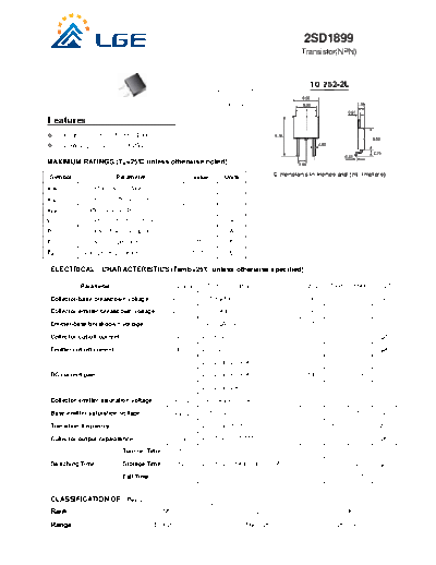
                                                                                                    2SD1899
                                                                                                   Transistor(NPN)

                                                                    1.BASE
                                                                                                      TO-252-2L
                                                                    2.COLLECTOR

                                                                    3.EMITTER


Features
       High hFE hFE=100 to 400
       Low VCE(sat) VCE(sat)=0.25V

MAXIMUM RATINGS (TA=25 unless otherwise noted)
                                                                                          Dimensions in inches and (millimeters)
 Symbol                    Parameter                       Value        Units
VCBO        Collector-Base Voltage                          60           V
VCEO        Collector-Emitter Voltage                       60           V
VEBO        Emitter-Base Voltage                            7            V
IC          Collector Current -Continuous                   3            A
PC          Collector Power Dissipation                     1            W
TJ          Junction Temperature                           150           
Tstg        Storage Temperature                           -55-150        

 ELECTRICAL CHARACTERISTICS (Tamb=25 unless otherwise specified)

            Parameter                           Symbol           Test    conditions                  MIN     TYP       MAX    UNIT

 Collector-base breakdown voltage               V(BR)CBO     IC=100A,IE=0                            60                        V

 Collector-emitter breakdown voltage            V(BR)CEO     IC =1mA,IB=0                            60                        V

 Emitter-base breakdown voltage                 V(BR)EBO     IE=100A,IC=0                             7                        V

 Collector cut-off current                        ICBO       VCB=60V,IE=0                                              10     A

 Emitter cut-off current                          IEBO       VEB=7V,IC=0                                               10     A

                                                 hFE(1)      VCE=2V,IC=200mA                         60

 DC current gain                                 hFE(2)      VCE=2V,IC=600mA                         100               400

                                                 hFE(3)      VCE=2V,IC=2A                            50

 Collector-emitter saturation voltage           VCE(sat)     IC=1.5A,IB=150mA                                          0.25    V

 Base-emitter saturation voltage                VBE(sat)     IC=1.5A,IB=150mA                                          1.2     V

 Transition frequency                              fT        VCE=5V,IC=1.5A                                  120              MHz

 Collector output capacitance                     Cob        VCB=10V,IE=0,f=1MHz                              30               pF

                             Turn on Time          ton                                                                 0.5

 Switching Time              Storage Time          tstg      VCC=10V,IC=1A,IB1=-IB2=-0.1A                              2.0     s

                             Fall Time              tf                                                                 0.5


 CLASSIFICATION OF            hFE(2)
 Rank                                       M                                         L                            K
 Range                                   100-200                                160-320                        200-400
                          2SD1899
                          Transistor(NPN)


Typical Characteristics
2SD1899
Transistor(NPN)


◦ Jabse Service Manual Search 2024 ◦ Jabse PravopisonTap.bg ◦ Other service manual resources online : FixyaeServiceinfo