Service Manuals, User Guides, Schematic Diagrams or docs for : . Electronic Components Datasheets Active components Transistors ST std3nb50-1
<< Back | HomeMost service manuals and schematics are PDF files, so You will need Adobre Acrobat Reader to view : Acrobat Download Some of the files are DjVu format. Readers and resources available here : DjVu Resources
For the compressed files, most common are zip and rar. Please, extract files with Your favorite compression software ( WinZip, WinRAR ... ) before viewing. If a document has multiple parts, You should download all, before extracting.
Good luck. Repair on Your own risk. Make sure You know what You are doing.
Image preview - the first page of the document
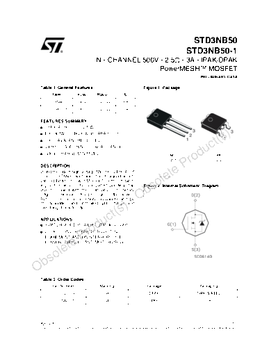
>> Download std3nb50-1 documenatation <<
Text preview - extract from the document
                                                                                                        STD3NB50
                                                                                                       STD3NB50-1
                                        N - CHANNEL 500V - 2.5 - 3A - IPAK/DPAK
                                                         PowerMESHTM MOSFET
                                                                                                                    PRELIMINARY DATA

 Table 1. General Features                                               Figure 1. Package
         Type             VDSS          RDS(on)            ID

     STD3NB50             500 V         < 2.8             3A
    STD3NB50-1            500 V         < 2.8             3A


 FEATURES SUMMARY
  TYPICAL RDS(on) = 2.5


                                                                                                                                s)
                                                                                                               3                       3
    EXTREMELY HIGH dv/dt CAPABILITY

                                                                                                                             t(
                                                                                                           2
    100% AVALANCHE TESTED                                                                              1                          1
    VERY LOW INTRINSIC CAPACITANCES
                                                                                                                    d uc
                                                                                                           ro
    GATE CHARGE MINIMIZED                                                               IPAK                              DPAK
                                                                                       TO-251                            TO-252


                                                                                          eP
 DESCRIPTION


                                                                                       let
 Using the latest high voltage MESH OVERLAYTM
 process, STMicroelectronics has designed an ad-

                                                                      so
 vanced family of power MOSFETs with outstand-
 ing performances. The new patent pending strip                          Figure 2. Internal Schematic Diagram

                                                                   Ob
 layout coupled with the Company's proprietary
 edge termination structure, gives the lowest
 RDS(on) per area, exceptional avalanche and dv/
                                                                 -
                                                   (s)
 dt capabilities and unrivalled gate charge and
 switching characteristics.

                                                ct
                                      du
 APPLICATIONS
  SWITCH MODE POWER SUPPLIES (SMPS)

                                    o
                        Pr
    DC-AC CONVERTERS FOR WELDING
    EQUIPMENT AND UNINTERRUPTIBLE
                      e
             let
    POWER SUPPLIES AND MOTOR DRIVE


           o
O bs
 Table 2. Order Codes
         Part Number                      Marking                          Package                                  Packaging
        STD3NB50T4                         D3NB50                            DPAK                                  TAPE & REEL
         STD3NB50-1                        D3NB50                             IPAK                                    TUBE


                                                                                                                       REV. 2
 April 2004                                                                                                                             1/8
 This is preliminary information on a new product now in development or undergoing evaluation. Details are subject to change without notice.
 STD3NB50/STD3NB50-1

 Figure 3. Absolute Maximum Ratings
       Symbol                            Parameter                               Value             Unit
         VDS       Drain-source Voltage (VGS = 0)                                500                V
        VDGR       Drain- gate Voltage (RGS = 20 k)                              500                V
         VGS       Gate-source Voltage
◦ Jabse Service Manual Search 2026 ◦ Jabse Pravopis ◦ onTap.bg ◦ Other service manual resources online : Fixya ◦ eServiceinfo