Service Manuals, User Guides, Schematic Diagrams or docs for : . Electronic Components Datasheets Active components Transistors ST stp80ne03l
<< Back | HomeMost service manuals and schematics are PDF files, so You will need Adobre Acrobat Reader to view : Acrobat Download Some of the files are DjVu format. Readers and resources available here : DjVu Resources
For the compressed files, most common are zip and rar. Please, extract files with Your favorite compression software ( WinZip, WinRAR ... ) before viewing. If a document has multiple parts, You should download all, before extracting.
Good luck. Repair on Your own risk. Make sure You know what You are doing.
Image preview - the first page of the document
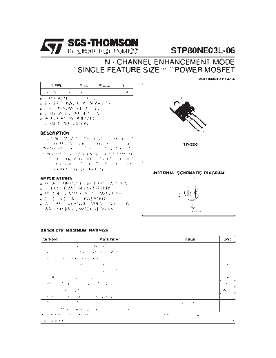
>> Download stp80ne03l documenatation <<
Text preview - extract from the document
                                                                                             STP80NE03L-06
                               N - CHANNEL ENHANCEMENT MODE
                       " SINGLE FEATURE SIZETM " POWER MOSFET
                                                                                                                 PRELIMINARY DATA
           T YPE            V DSS         R DS(o n)        ID
ST P80NE03L-06              30 V        < 0.006           80 A
s   TYPICAL RDS(on) = 0.005
s   EXCEPTIONAL dv/dt CAPABILITY
s   100% AVALANCHE TESTED
s   LOW GATE CHARGE 100 oC
s   APPLICATION ORIENTED
    CHARACTERIZATION
                                                                                                                         3
                                                                                                                     2
DESCRIPTION                                                                                                      1
This Power Mosfet is the latest development of
SGS-THOMSON unique "Single Feature Size"                                                              TO-220
strip-based process. The resulting transistor
shows extremely high packing density for low on-
resistance, rugged avalance characteristics and
less critical alignment steps therefore a remark-
able manufacturing reproducibility.
                                                                                INTERNAL SCHEMATIC DIAGRAM
APPLICATIONS
s HIGH CURRENT, HIGH SPEED SWITCHING
s SOLENOID AND RELAY DRIVERS
s MOTOR CONTROL, AUDIO AMPLIFIERS
s DC-DC & DC-AC CONVERTERS
s AUTOMOTIVE ENVIRONMENT (INJECTION,
  ABS, AIR-BAG, LAMPDRIVERS, Etc. )


ABSOLUTE MAXIMUM RATINGS
    Symbol                                 Parameter                                                   Value                         Uni t
     V DS      Drain-source Voltage (V GS = 0)                                                           30                           V
     V DGR     Drain- gate Voltage (R GS = 20 k)                                                         30                           V
     V GS      Gate-source Voltage
◦ Jabse Service Manual Search 2026 ◦ Jabse Pravopis ◦ onTap.bg ◦ Other service manual resources online : Fixya ◦ eServiceinfo