Service Manuals, User Guides, Schematic Diagrams or docs for : . Electronic Components Datasheets Active components Transistors Supertex tc2320
<< Back | HomeMost service manuals and schematics are PDF files, so You will need Adobre Acrobat Reader to view : Acrobat Download Some of the files are DjVu format. Readers and resources available here : DjVu Resources
For the compressed files, most common are zip and rar. Please, extract files with Your favorite compression software ( WinZip, WinRAR ... ) before viewing. If a document has multiple parts, You should download all, before extracting.
Good luck. Repair on Your own risk. Make sure You know what You are doing.
Image preview - the first page of the document
>> Download tc2320 documenatation <<
Text preview - extract from the document
TC2320
N- and P-Channel Enhancement-Mode Dual MOSFET
Features General Description
Low threshold The Supertex TC2320 consists of a high voltage, low
Low on-resistance threshold N- and P-channel MOSFET in an 8-Lead SOIC
Low input capacitance package. This low threshold enhancement-mode (normally-
Fast switching speeds off) transistor utilizes an advanced vertical DMOS structure
and Supertex's well-proven silicon-gate manufacturing
Freedom from secondary breakdown
process. This combination produces a device with the
Low input and output leakage
power handling capabilities of bipolar transistors and
Independent, electrically isolated N- and P-channels
with the high input impedance and positive temperature
coefficient inherent in MOS devices. Characteristic of all
Applications
MOS structures, this device is free from thermal runaway
Medical ultrasound transmitters and thermally-induced secondary breakdown.
High voltage pulsers
Amplifiers Supertex's vertical DMOS FETs are ideally suited to a
Buffers wide range of switching and amplifying applications where
Piezoelectric transducer drivers very low threshold voltage, high breakdown voltage, high
input impedance, low input capacitance, and fast switching
General purpose line drivers
speeds are desired.
Logic level interface
Ordering Information
BVDSS/BVDGS RDS(ON)
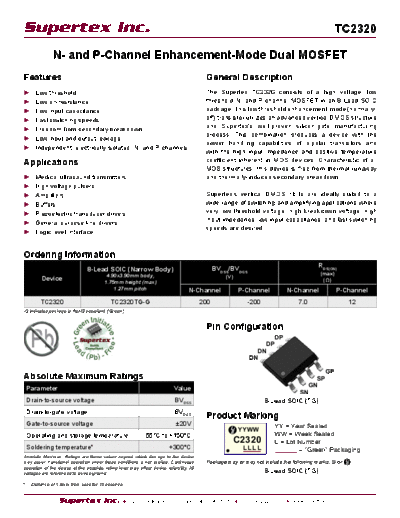
8-Lead SOIC (Narrow Body)
4.90x3.90mm body, (max)
Device (V)
1.75mm height (max) ()
1.27mm pitch N-Channel P-Channel N-Channel P-Channel
TC2320 TC2320TG-G 200 -200 7.0 12
-G indicates package is RoHS compliant (`Green')
Pin Configuration
DP
DP
DN
DN
GP
Absolute Maximum Ratings SP
Parameter Value GN
SN
Drain-to-source voltage BVDSS 8-Lead SOIC (TG)
Drain-to-gate voltage BVDGS
Product Marking
Gate-to-source voltage ◦ Jabse Service Manual Search 2026 ◦ Jabse Pravopis ◦ onTap.bg ◦ Other service manual resources online : Fixya ◦ eServiceinfo