Service Manuals, User Guides, Schematic Diagrams or docs for : . Electronic Components Datasheets Active components Transistors Philips bf1203
<< Back | HomeMost service manuals and schematics are PDF files, so You will need Adobre Acrobat Reader to view : Acrobat Download Some of the files are DjVu format. Readers and resources available here : DjVu Resources
For the compressed files, most common are zip and rar. Please, extract files with Your favorite compression software ( WinZip, WinRAR ... ) before viewing. If a document has multiple parts, You should download all, before extracting.
Good luck. Repair on Your own risk. Make sure You know what You are doing.
Image preview - the first page of the document
>> Download bf1203 documenatation <<
Text preview - extract from the document
                      DISCRETE SEMICONDUCTORS


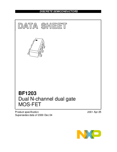
  DATA SHEET
 handbook, halfpage


                        MBD128


   BF1203
   Dual N-channel dual gate
   MOS-FET
Product specification                           2001 Apr 25
Supersedes data of 2000 Dec 04
NXP Semiconductors                                                                                            Product specification


  Dual N-channel dual gate MOS-FET                                                                                         BF1203

FEATURES                                                          PINNING - SOT363
 Two low noise gain controlled amplifiers in a single                   PIN                         DESCRIPTION
 package
                                                                         1             gate 1 (a)
 Superior cross-modulation performance during AGC
                                                                         2             gate 2
 High forward transfer admittance
                                                                         3             drain (a)
 High forward transfer admittance to input capacitance
                                                                         4             drain (b)
 ratio.
                                                                         5             source
                                                                         6             gate 1 (b)
APPLICATIONS
 Gain controlled low noise amplifiers for VHF and UHF
 applications with 3 to 9 V supply voltage, such as digital
 and analog television tuners and professional
 communications equipment.                                                                             g1 (b)          s   d (b)
                                                                  handbook, halfpage
                                                                           6     5      4

DESCRIPTION
The BF1203 is a combination of two different dual gate
                                                                                                         AMP               AMP
MOS-FET amplifiers with shared source and gate 2 leads.                                                   a                 b
The source and substrate are interconnected.
Internal bias circuits enable DC stabilization and a very                  1     2      3
good cross-modulation performance during AGC.                           Top view                         g1 (a)       g2   d (a)   MBL254

Integrated diodes between the gates and source protect
against excessive input voltage surges. The transistor is
                                                                     Marking code: L2-
encapsulated in a SOT363 micro-miniature plastic
package.
                                                                                Fig.1 Simplified outline and symbol.


QUICK REFERENCE DATA

 SYMBOL              PARAMETER                                CONDITIONS                            MIN.          TYP.     MAX. UNIT
Per MOS-FET unless otherwise specified
VDS           drain-source voltage                                                                                         10        V
ID            drain current (DC)                                                                                           30        mA
yfs           forward transfer admittance   amp. a: ID = 15 mA                                      23            28       35        mS
                                            amp. b: ID = 12 mA                                      25            30       40        mS
Cig1-s        input capacitance at gate 1   amp. a: ID = 15 mA; f = 1 MHz                                         2.6      3.1       pF
                                            amp. b: ID = 12 mA; f = 1 MHz                                         1.7      2.2       pF
Crss          reverse transfer capacitance f = 1 MHz                                                              15                 fF
NF            noise figure                  amp. a: f = 400 MHz; ID = 15 mA                                       1        1.8       dB
                                            amp. b: f = 800 MHz; ID = 12 mA                                       1.1      1.8       dB
Xmod          cross-modulation              amp. a: input level for k = 1% at 40 dB AGC 105                                          dBV
                                            amp. b: input level for k = 1% at 40 dB AGC 100                       105                dBV


                                                        CAUTION
 This product is supplied in anti-static packing to prevent damage caused by electrostatic discharge during transport
 and handling.

2001 Apr 25                                                   2
NXP Semiconductors                                                                               Product specification


  Dual N-channel dual gate MOS-FET                                                                     BF1203

LIMITING VALUES
In accordance with the Absolute Maximum Rating System (IEC 60134).
 SYMBOL                      PARAMETER                                 CONDITIONS      MIN.       MAX.         UNIT
Per MOS-FET unless otherwise specified
VDS                drain-source voltage                                                         10         V
ID                 drain current (DC)                                                           30         mA
IG1                gate 1 current                                                               10         mA
IG2                gate 2 current                                                               10         mA
Ptot               total power dissipation                    Ts  102 C; note 1                 200        mW
Tstg               storage temperature                                              65          +150       C
Tj                 operating junction temperature                                               150        C

Note
1. Ts is the temperature at the soldering point of the source lead.


THERMAL CHARACTERISTICS

 SYMBOL                                            PARAMETER                             VALUE            UNIT
Rth j-s            thermal resistance from junction to soldering point                    240              K/W


                                                      MGS359
        250
handbook, halfpage
       Ptot
      (mW)
        200


        150


        100


          50


          0
               0        50          100      150             200
                                                   Ts (
◦ Jabse Service Manual Search 2026 ◦ Jabse Pravopis ◦ onTap.bg ◦ Other service manual resources online : Fixya ◦ eServiceinfo