Service Manuals, User Guides, Schematic Diagrams or docs for : . Electronic Components Datasheets Active components Transistors Philips bf1206f
<< Back | HomeMost service manuals and schematics are PDF files, so You will need Adobre Acrobat Reader to view : Acrobat Download Some of the files are DjVu format. Readers and resources available here : DjVu Resources
For the compressed files, most common are zip and rar. Please, extract files with Your favorite compression software ( WinZip, WinRAR ... ) before viewing. If a document has multiple parts, You should download all, before extracting.
Good luck. Repair on Your own risk. Make sure You know what You are doing.
Image preview - the first page of the document
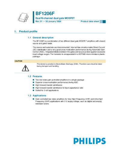
>> Download bf1206f documenatation <<
Text preview - extract from the document
                  BF1206F
                  Dual N-channel dual gate MOSFET
                  Rev. 01 -- 30 January 2006                                  Product data sheet


1. Product profile

          1.1 General description
              The BF1206F is a combination of two different dual gate MOSFET amplifiers with shared
              source and gate2 leads.

              The source and substrate are interconnected. Internal bias circuits enable Direct Current
              (DC) stabilization and a very good cross-modulation performance during Automatic Gain
              Control (AGC). Integrated diodes between the gates and source protect against excessive
              input voltage surges. The transistor is encapsulated in a SOT666 micro-miniature plastic
              package.

CAUTION
                   This device is sensitive to ElectroStatic Discharge (ESD). Therefore care should be taken
                   during transport and handling.


          1.2 Features
              s   Two low noise gain controlled amplifiers in a single package
              s   Superior cross-modulation performance during AGC
              s   High forward transfer admittance
              s   High forward transfer admittance to input capacitance ratio
              s   Suited for 3 volt applications

          1.3 Applications
              s Gain controlled low noise amplifiers for Very High Frequency (VHF) and Ultra High
                Frequency (UHF) applications with 3 V supply voltage, such as digital and analog
                television tuners
Philips Semiconductors                                                                                                BF1206F
                                                                                      Dual N-channel dual gate MOSFET


                     1.4 Quick reference data
                         Table 1: Quick reference data
                         Per MOSFET unless otherwise specified.
                         Symbol Parameter                           Conditions                               Min         Typ         Max Unit
                         VDS        drain-source voltage (DC)                                                -           -           6          V
                         ID         drain current (DC)                                                       -           -           30         mA
                         |yfs|      forward transfer admittance     ID = 4 mA
                                                                       amplifier A                           17          22          32         mS
                                                                       amplifier B                           17          22          32         mS
                         Ciss(G1)   input capacitance at gate1      ID = 4 mA; f = 100 MHz
                                                                       amplifier A                           -           2.4         2.9        pF
                                                                       amplifier B                           -           1.7         2.2        pF
                         NF         noise figure                    ID = 4 mA
                                                                       amplifier A; f = 400 MHz              -           1.0         1.6        dB
                                                                       amplifier B; f = 800 MHz              -           1.0         1.6        dB
                         Xmod       cross modulation                input level for k = 1 % at
                                                                    40 dB AGC
                                                                       amplifier A                           92          97          -          dB
◦ Jabse Service Manual Search 2026 ◦ Jabse Pravopis ◦ onTap.bg ◦ Other service manual resources online : Fixya ◦ eServiceinfo