Service Manuals, User Guides, Schematic Diagrams or docs for : . Electronic Components Datasheets Active components Transistors Wietron wt4410m

<< Back | Home

Most service manuals and schematics are PDF files, so You will need Adobre Acrobat Reader to view : Acrobat Download Some of the files are DjVu format. Readers and resources available here : DjVu Resources
For the compressed files, most common are zip and rar. Please, extract files with Your favorite compression software ( WinZip, WinRAR ... ) before viewing. If a document has multiple parts, You should download all, before extracting.
Good luck. Repair on Your own risk. Make sure You know what You are doing.


Image preview - the first page of the document
wt4410m


>> Download wt4410m documenatation <<

Text preview - extract from the document
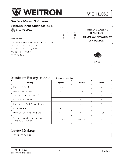
                                                                            WT4410M
Surface Mount N-Channel
Enhancement Mode MOSFET
 P b Lead(Pb)-Free                                                          DRAIN CURRENT


                                                               D
                                                       1
                                                   S


                                                           8
                                                                             10 AMPERS


                                                               D
                                                           7
                                                       2
                                                   S


                                                               D
                                                   S


                                                           6
                                                       3
                                                                         DRAIN SOUCE VOLTAGE
Features:


                                                               D
                                                   G
                                                       4


                                                           5
                                                                             30 VOLTAGE
*Super high dense cell design for low RDS(ON)
 R DS(ON) <11 m @VGS =10V
R DS(ON) <15 m  @VGS =4.5V
*Rugged and Reliable
*SO-8 Package
                                                                                  1

                                                                                SO-8


Maximum Ratings ( TA=25 C Unless Otherwise Specified)
                   Rating                       Symbol             Value              Unite
  Drain-Source Voltage                           VDS               30                   V
  Gate-Source Voltage                            VGS               +
                                                                   -20                  V
  Continuous Drain Current ( TJ =125 C) (1)       ID               10                   A
  Pulsed Drain Current (2)                       IDM               30                   A
  Drain-Source Diode Forward Current (1)          IS               2.3                  A

  Power Dissipation (1)                           PD               2.5                 W
  Maximax Junction-to-Ambient                    R JA              50                  C/W

  Operating Junction and Storage
                                                TJ, Tstg       -55 to 150               C
  Temperature Range


Device Marking
   W T4410M=SDM4410


     WEITRON                                     1/6                                   01-Jul-05
http://www.weitron.com.tw
       WT4410M
Electrical Characteristics                   (TA=25 C Unless otherwise noted)
                Characteristic                           Symbol        Min      Typ    Max         Unit
Static (2)
  Drain-Source Breakdown Voltage                           V(BR)DSS
  VGS=0V, ID=250 uA                                                    30        -      -           V
  Gate-Source Threshold Voltage                             VGS (th)                    3
  VDS=VGS, ID=250 uA                                                   1        1.5                 V
  Gate-Source Leakage Current                                IGSS                      +
              +                                                        -         -     -100         nA
  VDS=0V, VGS=-16V
  Zero Gate Voltage Drain Current                            IDSS      -         -      1           uA
  VDS=24V, VGS=0V
  Drain-Source On-Resistance                               rDS (on)                                m
  VGS=10V, ID=10A                                                       -        11    13.5
  VGS=4.5V, ID=5A                                                       -        15     20
  On-State Drain Current                                    ID(on)
  VDS=10V, VGS=10A                                                     40        -       -          A

  Forward Transconductance                                   gfs
  VDS=10V, ID=20A                                                      -          18     -          S

Dynamic (3)
  Input Capacitance                                          Ciss      -        1375     -
  VDS=15V, VGS=0V, f=1MHZ
  Output Capacitance                                                   -
  VDS=15V, VGS=0V, f=1MHZ
                                                             Coss                670     -          PF
  Reverse Transfer Capacitance
                                                            Crss       -         200        -
  VDS=15V, VGS=0V, f=1MHZ

Switching (3)
 Turn-On Delay Time
                                                            td(on)         -    30       -          nS
 VGS =10V,VDD =15V, I D =-1A, R GEN=6
 Rise Time
                                                              tr           -     32      -          nS
 VGS =10V,VDD =15V, I D =-1A, R GEN=6
 Turn-Off Time
                                                           td(off )        -    132      -           nS
  VGS =10V,VDD =15V, I D =-1A, R GEN=6
 Fall Time                                                                               -           nS
                                                              tf           -    30
 VGS =10V,VDD =15V, I D =-1A, R GEN=6
 Total Gate Charge                                            Qg                                     nc
 VDS=10V, ID=10A, VGS =10V                                                 -     40     50
 VDS=10V, ID=10A, V GS =4.5V                                               -     20     24
 Gate-Source Charge                                          Qgs                         -
                                                                           -    8.2                  nc
 VDS=10V, ID=10A, V GS =10V
 Gate-Drain Charge
                                                             Qgd           -    5.3      -           nc
 VDS=10V, ID=10A, V GS =10V
 Drain-Source Diode Forward Voltage
                                                              VSD          -    0.76    1.1          V
 VGS=0V, IS=2.3A

Note: 1. Surface Mounted on FR4 Board t < 10sec.
                                           _
      2. Pulse Test : PW < 300us, Duty Cycle < 2%.
                         _                   _
      3. Guaranteed by Design, not Subject to Production Testing.

     WEITRON                                                 2/6                                01-Jul-05
http://www.weitron.com.tw
           WT4410M                                                                                                                                                                                                                                                WE IT R ON
                                                                        25                                                                                                                             25
                                                                                                         VGS =10,9,8,7,6,5,4V
                                                                        20                                                                                                                             20


                                                                                                                                          ID , DRAIN CURRENT(A)
                                               ID ,DRAIN CURRENT(A)


                                                                                                                                                                                                                                                                     25 C

                                                                        15                                                                                                                             15


                                                                        10                                                                                                                             10                            Tj =125 C


                                                                            5                                                                                                                                        5
                                                                                                                       VGS =3V                                                                                                                               -55 C
                                                                            0                                                                                                                                        0
                                                                                0         0.5       1      1.5    2          2.5   3                                                                                  0.0         1.0     2.0    3.0        4.0   5.0     6.0
                                                                                VDS , DRAIN-TO-SOURCE VOLTAGE(V)                                                                                             VGS , GATE-TO-SOURCE VOLTAGE(V)

                                                                                    FIG.1. Output Characteristics                                                                                                         FIG.2 Transfer Characteristics

                                                                                                                                                                                                           0.030
                                                            1500                                                                                                                                                                        VGS =10V
                                                                                                                                                                                                           0.025
                                                                                                                                                             R DS(ON) , ON-RESISTANCE()
                        C ,CAPACITANCE( P F)


                                                            1200
                                                                                                                                                                                                           0.020
                                                                                                                                                                                                                                                       Tj =125 C
                                                                      900
                                                                                                                                                                                                           0.015
                                                                                                                                                                                                                                                                        25 C
                                                                      600                                             Ciss                                                                                 0.010
                                                                                                                                                                                                                                                                        -55 C
                                                                      300                                             Coss                                                                                 0.005
                                                                                                                      Crss
                                                                        0                                                                                                                                                 0
                                                                            0         5         10        15     20          25    30                                                                                         0            5           10         15            20
                                                                       VDS , DRAIN-TO-SOURCE VOLTAGE(V)                                                                                                                                  ID , DRAIN CURRENT(A)
                                                                                                                                                                                                                          FIG.4 On-Resistance Variation with
                                                                                      FIG.3 Capacitance
                                                                                                                                                                                                                                Drain Current and Temperature
                                                                                                                                                                                      DRAIN-SOURCE BREAKDOWN VOLTAGE(V)
                       GATE-SOURCE THRESHOLD VOLTAGE(V)


                                                                       1.09
                                                                                                                                                                                                                              1.15
                                                                       1.06                                           VDS =VGS                                                                                                          ID =-250uA
                                                                                                                      ID =250uA                                                                                               1.10
                                                                       1.03
     Vth ,NORMALIZED


                                                                                                                                                                                                                              1.05
                                                                                                                                                  BVDSS ,NORMALIZED


                                                                       1.00
                                                                                                                                                                                                                              1.00

                                                                       0.97
                                                                                                                                                                                                                              0.95
                                                                       0.94
                                                                                                                                                                                                                              0.90
                                                                       0.91                                                                                                                                                   0.85
                                                                          -50 -25               0       25 50    75 100 125 150                                                                                                  -50 -25 0         25 50 75 100 125 150

                                                                            T j ,JUNCTION TEMPERATURE( C)                                                                                                                         T j ,JUNCTION TEMPERATURE( C)

                                                                            FIG.5 Gate Threshold Variation                                                                                                                    FIG.6 Breakdown Voltage Variation
                                                                                  with Temperature                                                                                                                                  with Temperature


     WEITRON                                                                                                                            3/6                                                                                                                                          01-Jul-05
http://www.weitron.com.tw
                WT4410M                                                                                                                                                                                                       WE IT R ON
                                                                25                                                                                                          40.0


                                                                                                                                      IS ,SOURCE-DRAIN CURRENT(A)
    gFS ,TRANSCONDUCTANCE(S)


                                                                20


                                                                15                                                                                                          10.0


                                                                10


                                                                 5
                                                                                                          VDS =15V
                                                                0                                                                                                              1
                                                                     0              5            10            15         20                                                    0.4           0.6            0.8      1.0           1.2              1.4

                                                                         IDS ,DRAIN-SOURCE CURRENT(A)                                                                       V SD ,BODY DIODE FORWARD VOLTAGE(V)

                                                                 FIG.7 Transconductance Variation                                                                            FIG.8 Body Diode Forward Voltage
                                                                       with Drain Current                                                                                          Variation with Source Current

                                                                                                                                                                                 40                   it
                                                                         10                                                                                                                       im
                               VGS ,GATE TO SOURCE VOLTAGE(V)


                                                                                                                                                                                                 L
                                                                                                                                                                                              N)
                                                                                  VDS =10V                                                                                             (O
                                                                                                                                                    ID , DRAIN CURRENT(A)


                                                                                  ID =40A                                                                                        10 RDS
                                                                          8
                                                                                                                                                                                                                                    10m
                                                                                                                                                                                                                                          s
                                                                                                                                                                                                                              100
                                                                                                                                                                                                                                    ms
                                                                          6
                                                                                                                                                                                     1
                                                                                                                                                                                         1                                    1s

                                                                          4                                                                                                                                              DC


                                                                          2                                                                                                     0.1            VDS=10V
                                                                                                                                                                                               Single Pulse
                                                                                                                                                                              0.03             TC =25 C
                                                                          0
                                                                              0     5     10 15         20 25        30   35 40                                                   0.1                        1                     10            30 50

                                                                                  Q g ,TOTAL GATE CHARGE(nC)                                                                         VDS ,DRAIN-SOURCE CURRENT(V)

                                                                                                                                                                              FIG.10 Maximum Safe Operating Area
                                                                                         FIG.9 Gate Charge


                                                                                                              V DD
                                                                                                                                                                                                     ton                                  toff
                                                                                                                    RL                                                        td(on)                          tr    td(off)                           tf
                                                                                                 V IN                                                                                                        90%                               90%
                                                                                                          D                 V OUT
                                                                                                                                                                              V OUT                    10%     INVE R TE D                    10%
                                                                     VG S
                                                                                        R GE N     G
                                                                                                                                                                                                                                     90%
                                                                                                                                                                                                     50%                      50%
                                                                                                                                                                              V IN
                                                                                                          S                                                                          10%

                                                                                                                                                                                                           PULS E WIDTH


                                                                              FIG.11 Switching Test Circuit                                                                                  FIG.12 Switching Waveforms


        WEITRON                                                                                                                     4/6                                                                                                                    01-Jul-05
http://www.weitron.com.tw
                               WT4410M                                                                                                    WE IT R ON


                                                     10
  r(t) ,NORMALIZED TRANSIENT
                               THERMAL RESISTANCE


                                                           Duty Cycle=0.5

                                                      1
                                                             0.2

                                                             0.1                                                              P DM

                                                            0.05                                                                     t1
                                                     0.1                                                                                  t2

                                                            0.02                                                              1. R jA (t)=r (t) * R j A
                                                                                                                              2. R jA=See Datasheet
                                                                                                                              3. TjM-TA = PDM* R jA(t)
                                                                            Single Pulse                                      4. Duty Cycle, D=t1/t 2
                                                    0.01
                                                      0.00001        0.0001           0.001       0.01     0.1       1       10                100    1000


                                                                                           SQUARE WAVE PULSE DURATION(SEC)
                                                                        FIG.13 NORMALIZED THERMAL TRANSIENT IMPEDANCE CUREVE


                               WEITRON                                                                   5/6                                         01-Jul-05
http://www.weitron.com.tw
      WT4410M


SO-8 Package Outline Dimensions                                                Unit:mm


                  1
                                                                           
                                                                       L


                                                              E1
                                  D
                                                               7(4X)
                            7 (4X)
                                                 C
                                             A


                              e       B
                2A


                                          A1


                                                              eB


                                                 MILLIMETERS
                                      SYMBOLS
                                                 MIN      MAX
                                           A     1.35        1.75
                                          A1     0.10        0.20
                                           B     0.35        0.45
                                           C     0.18        0.23
                                           D     4.69        4.98
                                          E1     3.56        4.06
                                          eB     5.70        6.30
                                           e        1.27 BSC
                                           L     0.60        0.80
                                                  0           8


      WEITRON                                      6/6                        01-Jul-05
http://www.weitron.com.tw


◦ Jabse Service Manual Search 2024 ◦ Jabse PravopisonTap.bg ◦ Other service manual resources online : FixyaeServiceinfo