Service Manuals, User Guides, Schematic Diagrams or docs for : . Electronic Components Datasheets Active components Transistors Vishay si6926dq

<< Back | Home

Most service manuals and schematics are PDF files, so You will need Adobre Acrobat Reader to view : Acrobat Download Some of the files are DjVu format. Readers and resources available here : DjVu Resources
For the compressed files, most common are zip and rar. Please, extract files with Your favorite compression software ( WinZip, WinRAR ... ) before viewing. If a document has multiple parts, You should download all, before extracting.
Good luck. Repair on Your own risk. Make sure You know what You are doing.


Image preview - the first page of the document
si6926dq


>> Download si6926dq documenatation <<

Text preview - extract from the document
                                                                                                                   Si6926DQ
                                                                                                       Vishay Siliconix

                                   Dual N-Channel 2.5-V (G-S) MOSFET
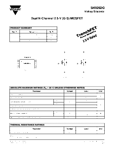

 PRODUCT SUMMARY
   VDS (V)                      rDS(on) (W)         ID (A)
                             0.035 @ VGS = 4.5 V    "4.0

      20                     0.040 @ VGS = 3.0 V    "3.7

                             0.045 @ VGS = 2.5 V    "3.5


                                                                         D1                          D2


                        TSSOP-8

        D1   1    D                       8   D2
        S1   2          Si6926DQ          7   S2             G1                          G2
        S1   3                            6   S2
        G1   4                            5   G2

                        Top View

                                                                         S1                          S2

                                                                  N-Channel MOSFET            N-Channel MOSFET


 ABSOLUTE MAXIMUM RATINGS (TA = 25_C UNLESS OTHERWISE NOTED)
                                     Parameter                                Symbol                   Limit                 Unit
 Drain-Source Voltage                                                          VDS                         20
                                                                                                                               V
 Gate-Source Voltage                                                           VGS                        "8

                                                             TA = 25_C                                    "4.0
 Continuous Drain Current (TJ = 150_C)a
                                150 C)                                          ID
                                                             TA = 70_C                                    "3.2
                                                                                                                               A
 Pulsed Drain Current                                                           IDM                       "20

 Continuous Source Current (Diode Conduction)a                                  IS                        1.25

                                                             TA = 25_C                                    1.0
 Maximum Power Dissipationa                                                     PD                                             W
                                                             TA = 70_C                                    0.64

 Operating Junction and Storage Temperature Range                             TJ, Tstg                


◦ Jabse Service Manual Search 2024 ◦ Jabse PravopisonTap.bg ◦ Other service manual resources online : FixyaeServiceinfo