Service Manuals, User Guides, Schematic Diagrams or docs for : . Electronic Components Datasheets Various 74LVC1G17
<< Back | HomeMost service manuals and schematics are PDF files, so You will need Adobre Acrobat Reader to view : Acrobat Download Some of the files are DjVu format. Readers and resources available here : DjVu Resources
For the compressed files, most common are zip and rar. Please, extract files with Your favorite compression software ( WinZip, WinRAR ... ) before viewing. If a document has multiple parts, You should download all, before extracting.
Good luck. Repair on Your own risk. Make sure You know what You are doing.
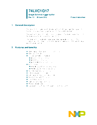
Image preview - the first page of the document

>> Download 74LVC1G17 documenatation <<
Text preview - extract from the document
                 74LVC1G17
                 Single Schmitt trigger buffer
                 Rev. 10 -- 29 June 2012                                          Product data sheet


1. General description
              The 74LVC1G17 provides a buffer function with Schmitt trigger input. It is capable of
              transforming slowly changing input signals into sharply defined outputs.

              The input can be driven from either 3.3 V or 5 V devices. This feature allows the use of
              this device in a mixed 3.3 V and 5 V environment.

              This device is fully specified for partial power-down applications using IOFF. The IOFF
              circuitry disables the output, preventing the damaging backflow current through the device
              when it is powered down.


2. Features and benefits
               Wide supply voltage range from 1.65 V to 5.5 V
               High noise immunity
               Complies with JEDEC standard
                 JESD8-7 (1.65 V to 1.95 V)
                 JESD8-5 (2.3 V to 2.7 V)
                 JESD8B/JESD36 (2.7 V to 3.6 V)
               ESD protection:
                 HBM JESD22-A114F exceeds 2000 V
                 MM JESD22-A115-A exceeds 200 V
               24 mA output drive (VCC = 3.0 V)
               CMOS low power consumption
               Latch-up performance exceeds 250 mA
               Direct interface with TTL levels
               Unlimited rise and fall times
               Inputs accept voltages up to 5 V
               Multiple package options
               Specified from 40 C to +85 C and from 40 C to +125 C
NXP Semiconductors                                                                                                                     74LVC1G17
                                                                                                                                  Single Schmitt trigger buffer


3. Ordering information
Table 1.      Ordering information
Type number                 Package
                            Temperature range                 Name                      Description                                                           Version
74LVC1G17GW                 40 C to +125 C                    TSSOP5                    plastic thin shrink small outline package;                            SOT353-1
                                                                                        5 leads; body width 1.25 mm
74LVC1G17GV                 40 C to +125 C                    SC-74A                    plastic surface-mounted package; 5 leads                              SOT753
74LVC1G17GM                 40 C to +125 C                    XSON6                     plastic extremely thin small outline package;                         SOT886
                                                                                        no leads; 6 terminals; body 1  1.45  0.5 mm
74LVC1G17GF                 40 C to +125 C                    XSON6                     plastic extremely thin small outline package;                         SOT891
                                                                                        no leads; 6 terminals; body 1  1  0.5 mm
74LVC1G17GN                 40 C to +125 C                    XSON6                     extremely thin small outline package; no leads; SOT1115
                                                                                        6 terminals; body 0.9  1.0  0.35 mm
74LVC1G17GS                 40 C to +125 C                    XSON6                     extremely thin small outline package; no leads; SOT1202
                                                                                        6 terminals; body 1.0  1.0  0.35 mm
74LVC1G17GX                 40 C to +125 C                    X2SON5                    X2SON5: plastic thermal enhanced extremely                            SOT1226
                                                                                        thin small outline package; no leads; 5
                                                                                        terminals; body 0.8  0.8  0.35 mm


4. Marking
Table 2.      Marking codes
Type number                                                                           Marking[1]
74LVC1G17GW                                                                           VJ
74LVC1G17GV                                                                           V17
74LVC1G17GM                                                                           VJ
74LVC1G17GF                                                                           VJ
74LVC1G17GN                                                                           VJ
74LVC1G17GS                                                                           VJ
74LVC1G17GX                                                                           VJ

[1]   The pin 1 indicator is located on the lower left corner of the device, below the marking code.


5. Functional diagram


                            A              Y
                       2                         4
                                                                                                                              2            4

                                       mnb150                                                                                         mnb151


  Fig 1.    Logic symbol                                                                Fig 2.           IEC logic symbol


74LVC1G17                                        All information provided in this document is subject to legal disclaimers.
◦ Jabse Service Manual Search 2024 ◦ Jabse Pravopis ◦ onTap.bg ◦ Other service manual resources online : Fixya ◦ eServiceinfo