Service Manuals, User Guides, Schematic Diagrams or docs for : . Electronic Components Datasheets Various ta7678
<< Back | HomeMost service manuals and schematics are PDF files, so You will need Adobre Acrobat Reader to view : Acrobat Download Some of the files are DjVu format. Readers and resources available here : DjVu Resources
For the compressed files, most common are zip and rar. Please, extract files with Your favorite compression software ( WinZip, WinRAR ... ) before viewing. If a document has multiple parts, You should download all, before extracting.
Good luck. Repair on Your own risk. Make sure You know what You are doing.
Image preview - the first page of the document
>> Download ta7678 documenatation <<
Text preview - extract from the document
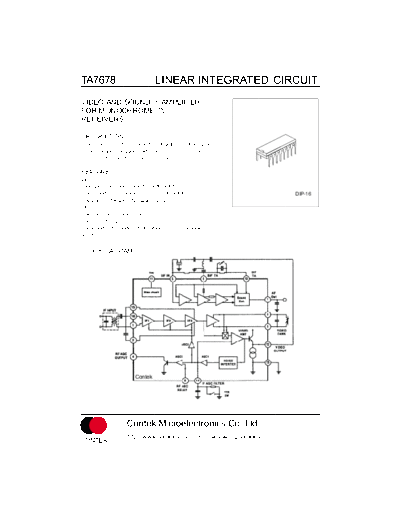
TA7678                               LINEAR INTEGRATED CIRCUIT
VIDEO AND SOUND IF AMPLIFIER
FOR MONOCHROME TV
RECEIVERS

DESCRIPTION
 The Contek TA7678 is a monolithic integrated circuit designed
for the VIF and SIF stage in B/W television receivers. The
UTC TA7678 is used for forward AGC Type.


FEATURE
VIF STAGE
*High gain wide brand IF amplifier 50dB at 45MHz
*Gain reduction with excellent stability: 55dB at 45MHz                       DIP-16
*Excellent DG/DP and S/N characteristics
SIF STAGE
*Excellent limiter characteristics
*Excellent AM Rejection
*Large undistorted audio output voltage with       quadrature
detector


BLOCK DIAGRAM


                            Contek


                        Contek Microelectronics Co.,Ltd.                               1

                        http://www.contek-ic.com E-mail:[email protected]
CONTEK
TA7678                                       LINEAR INTEGRATED CIRCUIT
ABSOLUTE MAXIMUM RATINGS (Ta=25                                  C)
                         PARAMETER                   SYMBOL                       VALUE                       UNIT
Supply Voltage                                           Vcc                         15                            V
Open Loop Voltage                                         V4                         15                            V
Video DC output current (note)                           V12                         6                             V
Operating Temperature                                   Topr                     -20 to +65                        C
Storage Temperature                                      Tstg                    -55 to 155                        C
Power dissipation                                         PD                        1.4                            W

ELECTRICAL CHARACTERISTICS(Ta=25                                  C,Vcc=12V,fp=45.75MHz,unless otherwise specified)
                   PARAMETER                   TEST      SYMBOL          TEST CONDITIONS       MIN. TYP. MAX. UNIT
                                              CIRCUIT
Recommended Supply Voltage                              Vcc                                     10.8   12    13.2        V
Quiescent circuit current                        1      Iccq           S1:ON,S3:2,S5:2,S4:1     35     50    65         mA
Video DC output                                  1      V12            S1:OFF,S3:2,S5:2,S4:1    5.2    5.5   5.8         V
Terminal 5 voltage                               1      V5             S1:ON,S3:2,S5:2,S4:1     3.5    4.4   5.3         V
Terminal 7 voltage                               1      V5             S1:ON,S3:2,S5:2,S4:1     4.6    6.0   7.2         V
RF AGC Residual Output Voltage                   1      V4(sat)        S1:OFF,S3:2,S5:2,S4:1                 0.5         V
RF AGC Leak Current                              1      I4(leak)       S1:OFF,S3:1,S5:2,S4:1                  1         mA
Video sensitivity                                2      SVI            Note 1                   60     150   250       mVrms
AGC Range                                        2      VAGC(IF)       Note 2                   60     64               dB
Sync Tip Level Voltage (pin12)                   2      Vsync          Note 3                   2.3    2.5   2.7         V
                                                        (pin12)
Maximum IF Input Voltage                         2      VI(MAX)        Note 4                   100    120             mVrms
White Noise Threshold (pin12)                    2      VWTH           Note 5                   5.8    6.2   6.6         V
                                                        (pin12)
White Noise Clamp Level (pin12)                  2      VWCL           Note 5                   3.7    4.1   4.5         V
                                                        (pin12)
Black Noise Threshold (pin12)                    2      VBTH           Note 5                   1.4    1.6   1.8         V
                                                        (pin12)
Black Noise Clamp Level (pin12)                  2      VBCL(pin12)    Note 5                   2.9    3.3   3.7         V


Video Frequency Response                         3      Gv(IF)         Note 6                   4.5    5.5             MHz


Suppression of carrier                           4      CL             Note 7                   40     50               dB

                           nd
Suppression of 2                Carrier          4      I2nd           Note 8                   40     50               dB
920kHz Beat level                                4      I920           Note 9                   33     38               dB
Differentital Gain                               5      DG             Note 10                          7    10         dB
Differential Phase                               5      DP             Note 10                         3.5    5          C
VIF Input Impedance                              6      RIN            Note 11                  1.5    3.0   6.0         k
                                                        CIN                                            3.0   10.0       pF
Maximum Avaliable Current                        1      I4(MAX)        Note 12                   7                      mA
RF AGC delay Point Range                         2      Vin(delay)     Note 13                  5.0    7.0   9.0         V
Video output level                               2      Vo0            Note 14                  2.25   2.5   2.75        V


                                    Contek Microelectronics Co.,Ltd.                                                         2

                                    http://www.contek-ic.com E-mail:[email protected]
CONTEK
TA7678                                LINEAR INTEGRATED CIRCUIT
SIF STAGE           (Ta=25 C,Vcc=12V,fo=45.75MHz,unless otherwise specified)
          PARAMETER                     TEST       SYMBOL        TEST CONDITIONS          MIN. TYP. MAX. UNIT
                                       CIRCUIT
SIF Output Voltage                        3           VSO      Note 15                    200   400    600   mVrms
Input limiting voltage                    8          Vi(lim)   Note 16                    200   400          mVrms
AM Rejection Ratio                        8           AMR      Note 17                    40    45            dB
Recovered Output Voltage                  8           VOD      Note 18                    0.5   0.75         Vrms
Total Harmonic distortion                 8           THD      Note 18                          1.0    2.0       %
Maximun Audi Output Voltage               8          VOM       Noet 19                    4.0                Vp-p
SIF Input Impedance                       7         RIN(SIF)                              10    20     30     kW
                                                    CIN(SIF)                                     3     10     pF
Audio Output Impedance                    9         RO(AF)     Note 20                    10    15     20     kW


Note:
1.   VAGC=11.5V,VIF Input : 45.5MHz,1kHz,30 AM Modulation. Adjust VIF input Vi level so that the detected output of
     Pin 12 with high impedance probe will be 0.8Vp-p and measure the input Level.
2.   VAGC=4V. Measure VIF input level vi is same as note 1 DA=20log(Vi /Vi)(dB)
3.   VIF input : f=45.75MHz CW 15mVrms. Measure the DC level of Pin12.
4.   VIF Input : f=45.75MHz APL 100%.87.5% AM Modulation. Pin 14 Open
     4.1. Adjust VIF inpt level 50mVp-p and measure the detected output level Vo(p-p)
     4.2. Then increase the input level so that the detected output level will be 1.1* Vo(p-p) and measure the input
           level.
5.   VAGC=8V. VIF input : f=45.75MHz+-10MHz variable or sweep 15mVrms measure DC level of Pin12.


6.   VAGC=8V. SG1:45.75MHz CW. SG2:45.65~27MHz variable.
     6.1. Setting output of SG1 s o that the DC level of Pin12 will be
     6.2. Setting output of SG1(45.65MHz so that the AC level of Pin12 will be 0.5Vp-p.
     6.3. Decreasing frequency of SG2 until the AC level of Pin 12 will be 0.35vp-p(-3dB of 0.5Vp-p) then read
           FSG2=F, fBW=45.75-F MHZ
7.   SG1:45.75MHz, 1kHz 80% AM Modulation 100mVrms. SG2 ,SG3:OFF. Setting VAGC so that the output AC
     level of Pin12 will be 2.7Vp-p. Measure CL of Pin12 after setting to 0% AM of SG1.
                 nd
8.   Measure 2      of Pin12 same as note 9.


                         Contek Microelectronics Co.,Ltd.                                                            3

                         http://www.contek-ic.com E-mail:[email protected]
CONTEK
TA7678                                LINEAR INTEGRATED CIRCUIT
9.    VAGC=8V. SG1 :45.75MHz(P:picture) 100mVrms, SG2:41.25MHz(S: Sound) 32mVrms(-10dB of
      SG1),SG3:42.17MHz(C:Chroma) 32mVrms(-10dB of SG1)
      9.1. Setting VAGC so that the output Pin12 will be 3.0V DC.
      9.2. Measure the level difference between the C-level and 920kHz.
10.   VAGC=8V. VIF Input : f=45.75MHz video signal (RAMP) 87.5% AM 100mVp-p. Setting ATT so that the SYNC TIP
      level of Pin12 will be 2.5VDC measure DP and DG.
11.   VAGC=5V. f=45.75MHz. Measure RIN and CIN.
12.   S1=ON, S3=2,S5=1,S4=2
13.   Pin 14 open. VIF Input : 45.75MHz CW 20mVrms.
      13.1. Adjust the voltate of Pin 3 so that the voltage of Pin4 will be 6.0V DC.
      13.2. Measure the Pin 3.
14.   Pin 14 open. VIF Input: 45 .75MHz 100% APL 87.5% AM Modulation signal amplitude 50mVp-p               mesure the
      detected output voltage (white peak to SYNC TIP)
15.   PIN14: Op en. SG1 :45.75MHz CW 100mvrms. SG2 :41.25MHz CW 25mVrms. Measre SIF(4.5MHz) output
      voltage at Pin12.
16.   SIF input: f=4.5MHz FM fMOD=400Hzm           Df=+-25kHz
      16.1. Adjust SIF input level 100mVp-p and measure the detected output level Vos.
      16.2. Then decrease the i nput level so that the detected output level will be 3dB down of   Vos and measure the
           input level.
17.   SIF input: f=4.5MHz, FM fMOD=400Hz         Df=+-25kHz. AM 30%,input level Vins=80dB m.
18.   SIF input: f=4.5MHz, fM fMOD=400Hz        Df=+-25kHz. Input level Vins=80dB m
19.   SIF input: f=4.4~4.6MHz variable or sweep measure the outjput DC voltage change.
20.   SIF inptut : f=4.5MHz, FM FMOD=400Hz         Df=+-25kHz, input level Vins=80dB m.
      20.1. Measure the detected output voltagae vOA with Rx= .
      20.2. Then, adjust Rx so that the d etected output voltage will be VOA/2 and measure Rx.


1. DC TEST CIRCUIT


                          Contek Microelectronics Co.,Ltd.                                                          4

                          http://www.contek-ic.com E-mail:[email protected]
CONTEK
TA7678                 LINEAR INTEGRATED CIRCUIT
2. AC TESTS CIRCUIT


3. VIDEO FREQUENCY RESPONSE & SIF OUTPUT VOLTAGE TEST CIRCUIT


4.   INTER MODULATION TEST CIRCUIT


             Contek Microelectronics Co.,Ltd.                       5

              http://www.contek-ic.com E-mail:[email protected]
CONTEK
TA7678                  LINEAR INTEGRATED CIRCUIT
5. DG,DP TEST CIRCUIT


5.   INPUT IMPEDANCE TEST CIRCUIT


             Contek Microelectronics Co.,Ltd.                       6

              http://www.contek-ic.com E-mail:[email protected]
CONTEK
TA7678                  LINEAR INTEGRATED CIRCUIT
7. SIF INPUT IMPEDANCE TEST CIRCUIT


8. VIN(LIM) AMR, VOD,THD VOM TEST CIRCUIT


9. AUDIO OUTPUT IMPEDANCE TEST CIRCUIT


UTC            UNISONIC TECHNOLOGIES CO., LTD.   7
TA7678                LINEAR INTEGRATED CIRCUIT
TYPICAL APPLICATION CIRCUIT


            Contek Microelectronics Co.,Ltd.                       8

             http://www.contek-ic.com E-mail:[email protected]
CONTEK
◦ Jabse Service Manual Search 2026 ◦ Jabse Pravopis ◦ onTap.bg ◦ Other service manual resources online : Fixya ◦ eServiceinfo