Service Manuals, User Guides, Schematic Diagrams or docs for : . Electronic Components Datasheets Various AOD412
<< Back | HomeMost service manuals and schematics are PDF files, so You will need Adobre Acrobat Reader to view : Acrobat Download Some of the files are DjVu format. Readers and resources available here : DjVu Resources
For the compressed files, most common are zip and rar. Please, extract files with Your favorite compression software ( WinZip, WinRAR ... ) before viewing. If a document has multiple parts, You should download all, before extracting.
Good luck. Repair on Your own risk. Make sure You know what You are doing.
Image preview - the first page of the document
>> Download AOD412 documenatation <<
Text preview - extract from the document
AOD412
N-Channel Enhancement Mode Field Effect Transistor
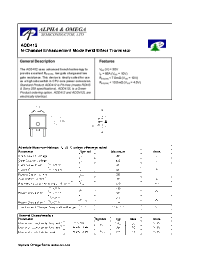
General Description Features
The AOD412 uses advanced trench technology to VDS (V) = 30V
provide excellent RDS(ON), low gate chargeand low ID = 85A (VGS = 10V)
gate resistance. This device is ideally suited for use RDS(ON) < 7.0m (VGS = 10V)
as a high side switch in CPU core power conversion. RDS(ON) < 10.5m (VGS = 4.5V)
Standard Product AOD412 is Pb-free (meets ROHS
& Sony 259 specifications). AOD412L is a Green
Product ordering option. AOD412 and AOD412L are
electrically identical.
TO-252
D-PAK
D
Top View
Drain Connected
to Tab
G
S
G D S
Absolute Maximum Ratings TA=25◦ Jabse Service Manual Search 2026 ◦ Jabse Pravopis ◦ onTap.bg ◦ Other service manual resources online : Fixya ◦ eServiceinfo