Service Manuals, User Guides, Schematic Diagrams or docs for : . Electronic Components Datasheets Various AP85t03gh

<< Back | Home

Most service manuals and schematics are PDF files, so You will need Adobre Acrobat Reader to view : Acrobat Download Some of the files are DjVu format. Readers and resources available here : DjVu Resources
For the compressed files, most common are zip and rar. Please, extract files with Your favorite compression software ( WinZip, WinRAR ... ) before viewing. If a document has multiple parts, You should download all, before extracting.
Good luck. Repair on Your own risk. Make sure You know what You are doing.


Image preview - the first page of the document
AP85t03gh


>> Download AP85t03gh documenatation <<

Text preview - extract from the document
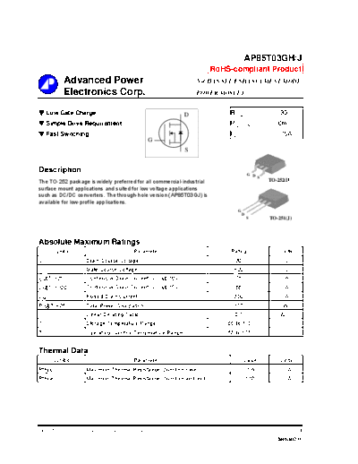
                                                                                     AP85T03GH/J
                                                                       RoHS-compliant Product
           Advanced Power                                       N-CHANNEL ENHANCEMENT MODE
           Electronics Corp.                                    POWER MOSFET


 Low Gate Charge                                            D               BVDSS                    30V
 Simple Drive Requirement                                                   RDS(ON)                 6m
 Fast Switching                                                             ID                       75A
                                                 G
                                                            S


Description                                                                              G D
                                                                                             S
The TO-252 package is widely preferred for all commercial-industrial                             TO-252(H)
surface mount applications and suited for low voltage applications
such as DC/DC converters. The through-hole version (AP85T03GJ) is
available for low-profile applications.
                                                                                 G
                                                                                     D
                                                                                         S       TO-251(J)


Absolute Maximum Ratings
       Symbol                             Parameter                         Rating                   Units
VDS                  Drain-Source Voltage                                    30                        V
VGS                  Gate-Source Voltage                                     +20                       V
ID@TC=25             Continuous Drain Current, VGS @ 10V                     75                        A
ID@TC=100            Continuous Drain Current, VGS @ 10V                     55                        A
                                            1
IDM                  Pulsed Drain Current                                    350                       A
PD@TC=25             Total Power Dissipation                                 107                      W
                     Linear Derating Factor                                  0.7                     W/
TSTG                 Storage Temperature Range                            -55 to 175                  
TJ                   Operating Junction Temperature Range                 -55 to 175                  


Thermal Data
       Symbol                             Parameter                                  Value           Units
Rthj-c               Maximum Thermal Resistance, Junction-case                           1.4         /W
Rthj-a               Maximum Thermal Resistance, Junction-ambient                        110         /W


Data & specifications subject to change without notice                                                       1
                                                                                                    200810235
AP85T03GH/J

Electrical Characteristics@Tj=25oC(unless otherwise specified)
       Symbol                 Parameter                            Test Conditions   Min.   Typ.   Max. Units
BVDSS           Drain-Source Breakdown Voltage            VGS=0V, ID=250uA           30      -      -     V
BVDSS/Tj        Breakdown Voltage Temperature Coefficient Reference to 25, ID=1mA     -     0.02    -     V/
                                                      2
RDS(ON)         Static Drain-Source On-Resistance         VGS=10V, ID=45A             -      -      6     m
                                                          VGS=4.5V, ID=30A            -      -      10    m
VGS(th)         Gate Threshold Voltage                    VDS=VGS, ID=250uA           1      -      3     V
gfs             Forward Transconductance                  VDS=10V, ID=30A             -     55      -     S
IDSS            Drain-Source Leakage Current              VDS=30V, VGS=0V             -      -      1     uA
                                                      o
                Drain-Source Leakage Current (T j=175 C) VDS=24V, VGS=0V              -      -     500    uA
IGSS            Gate-Source Leakage                       VGS=+20V                    -      -     +100   nA
                                    2
Qg              Total Gate Charge                         ID=30A                      -     33      52    nC
Qgs             Gate-Source Charge                        VDS=24V                     -      8            nC
Qgd             Gate-Drain ("Miller") Charge              VGS=4.5V                    -     24            nC
Qoss            Output Charge                             VDD=15V,VGS=0V              -     24.5    39    nC
                                        2
td(on)          Turn-on Delay Time                        VDS=15V                     -     11      -     ns
tr              Rise Time                                 ID=30A                      -     77      -     ns
td(off)         Turn-off Delay Time                       RG=3.3,VGS=10V              -     35      -     ns
tf              Fall Time                                 RD=0.5                      -     67      -     ns
Ciss            Input Capacitance                         VGS=0V                      -     2700 4200     pF
Coss            Output Capacitance                        VDS=25V                     -     550     -     pF
Crss            Reverse Transfer Capacitance              f=1.0MHz                    -     380     -     pF


Source-Drain Diode
       Symbol                 Parameter                            Test Conditions   Min.   Typ.   Max. Units
                                        2
VSD             Forward On Voltage                        IS=45A, VGS=0V              -      -     1.3    V
                                            2
trr             Reverse Recovery Time                     IS=30A, VGS=0V,             -     28      -     ns
Qrr             Reverse Recovery Charge                   dI/dt=100A/


◦ Jabse Service Manual Search 2024 ◦ Jabse PravopisonTap.bg ◦ Other service manual resources online : FixyaeServiceinfo