Service Manuals, User Guides, Schematic Diagrams or docs for : . Electronic Components Datasheets Various SUD50N024-09P - N-Channel 22-V (D-S) 175C MOSFET
<< Back | HomeMost service manuals and schematics are PDF files, so You will need Adobre Acrobat Reader to view : Acrobat Download Some of the files are DjVu format. Readers and resources available here : DjVu Resources
For the compressed files, most common are zip and rar. Please, extract files with Your favorite compression software ( WinZip, WinRAR ... ) before viewing. If a document has multiple parts, You should download all, before extracting.
Good luck. Repair on Your own risk. Make sure You know what You are doing.
Image preview - the first page of the document
>> Download SUD50N024-09P - N-Channel 22-V (D-S) 175C MOSFET documenatation <<
Text preview - extract from the document
SUD50N024-09P
Vishay Siliconix
N-Channel 22-V (D-S) 175_C MOSFET
FEATURES
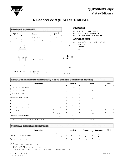
PRODUCT SUMMARY
D TrenchFETr Power MOSFET
VDS (V) rDS(on) (W) ID (A)d D 175_C Junction Temperature
D PWM Optimized for High Efficiency
0.0095 @ VGS = 10 V 49
24c APPLICATIONS
0.017 @ VGS = 4.5 V 36
D High-Side Synchronous Buck DC/DC
D Conversion
TO-252
- Desktop
- Server
G
Drain Connected to Tab
G D S
Top View
S
Ordering Information: SUD50N024-09P
SUD50N024-09P--E3 (Lead Free) N-Channel MOSFET
ABSOLUTE MAXIMUM RATINGS (TA = 25_C UNLESS OTHERWISE NOTED)
Parameter Symbol Limit Unit
Drain-Source Pulse Voltage VDS(pulse) 24C
Drain-Source Voltage VDS 22 V
Gate-Source Voltage VGS "20
TC = 25_C 49d
Continuous Drain Currenta ID
TC= 100_C 34d
Pulsed Drain Current IDM 100 A
Continuous Source Current (Diode Conduction)a IS 4.3
Avalanche Current, Single Pulse L = 0.1 mH IAS 29
Avalanche Energy, Single Pulse EAS 42 mJ
TA = 25_C 6.5a
Maximum Power Dissipation PD W
TC = 25_C 39.5
Operating Junction and Storage Temperature Range TJ, Tstg -55 to 175 _C
THERMAL RESISTANCE RATINGS
Parameter Symbol Typical Maximum Unit
t v 10 sec 19 23
Maximum Junction to Ambienta
Junction-to-Ambient RthJA
Steady State 40 50 C/W
_C/W
Maximum Junction-to-Case RthJC 3.1 3.8
Notes
a. Surface Mounted on FR4 Board, t v 10 sec.
b. Limited by package
c. Pulse condition: TA = 105_C, 50 ns, 300 kHz operation
d. Calculation based on maximum allowable Junction Temperature. Package limitation current is 25 A.
Document Number: 72290 www.vishay.com
S-41168--Rev. B, 14-Jun-04 1
SUD50N024-09P
Vishay Siliconix
SPECIFICATIONS (TJ = 25_C UNLESS OTHERWISE NOTED)
Parameter Symbol Test Condition Min Typa Max Unit
Static
Drain-Source Breakdown Voltage V(BR)DSS VGS = 0 V, ID = 250 mA 22
V
Gate Threshold Voltage VGS(th) VDS = VGS, ID = 250 mA 0.8 3.0
Gate-Body Leakage IGSS VDS = 0 V, VGS = "20 V "100 nA
VDS = 20 V, VGS = 0 V 1
Zero Gate Voltage Drain Current IDSS mA
VDS = 20 V, VGS = 0 V, TJ = 125_C 50
On-State Drain Currentb ID(on) VDS = 5 V, VGS = 10 V 50 A
VGS = 10 V, ID = 20 A 0.008 0.0095
Drain-Source On-State Resistanceb
Drain Source On State rDS(on) VGS = 10 V, ID = 20 A, TJ = 125_C 0.014 W
VGS = 4.5 V, ID = 20 A 0.0135 0.017
Forward Transconductanceb gfs VDS = 15 V, ID = 20 A 15 S
Dynamica
Input Capacitance Ciss 1300
Output Capacitance Coss VGS = 0 V, VDS = 10 V, f = 1 MHz 470 p
pF
Reverse Transfer Capacitance Crss 275
Gate Resistance Rg 1.6 4.0 6 W
Total Gate Chargec Qg 10.5 16
Gate-Source Chargec Qgs VDS = 10 V, VGS = 4.5 V, ID = 50 A 4.2 nC
Gate-Drain Chargec Qgd 4.0
Turn-On Delay Timec td(on) 8 12
Rise Timec tr VDD = 10 V, RL = 0.2 W 10 15
ns
Turn-Off Delay Timec td(off) ID ^ 50 A, VGEN = 10 V, Rg = 2.5 W 25 40
Fall Timec tf 12 20
Source-Drain Diode Ratings and Characteristic (TC = 25_C)
Pulsed Current ISM 100 A
Diode Forward Voltageb VSD IF = 50 A, VGS = 0 V 1.2 1.5 V
Source-Drain Reverse Recovery Time trr IF = 50 A, di/dt = 100 A/ms 35 70 ns
Notes
a. Guaranteed by design, not subject to production testing.
b. Pulse test; pulse width v 300 ms, duty cycle v 2%.
c. Independent of operating temperature.
TYPICAL CHARACTERISTICS (25_C UNLESS NOTED)
Output Characteristics Transfer Characteristics
100 100
VGS = 10 thru 6 V
TC = -55_C
5V
80 80
25_C
I D - Drain Current (A)
I D - Drain Current (A)
60 60
4V 125_C
40 40
20 20
3V
0 0
0 2 4 6 8 10 0 1 2 3 4 5 6
VDS - Drain-to-Source Voltage (V) VGS - Gate-to-Source Voltage (V)
www.vishay.com Document Number: 72290
2 S-41168--Rev. B, 14-Jun-04
SUD50N024-09P
Vishay Siliconix
TYPICAL CHARACTERISTICS (25_C UNLESS NOTED)
Transconductance On-Resistance vs. Drain Current
60 0.030
TC = -55_C
50 0.025
r DS(on)- On-Resistance ( W )
25_C
VGS = 4.5 V
g fs - Transconductance (S)
40 0.020
125_C
30 0.015
20 0.010 VGS = 10 V
10 0.005
0 0.000
0 10 20 30 40 50 0 20 40 60 80 100
ID - Drain Current (A) ID - Drain Current (A)
Capacitance Gate Charge
2000 10
VDS = 10 V
V GS - Gate-to-Source Voltage (V)
1600 8 ID = 50 A
Ciss
C - Capacitance (pF)
1200 6
800 4
Coss
400 2
Crss
0 0
0 4 8 12 16 20 0 4 8 12 16 20
VDS - Drain-to-Source Voltage (V) Qg - Total Gate Charge (nC)
On-Resistance vs. Junction Temperature Source-Drain Diode Forward Voltage
1.8 100
VGS = 10 V
ID = 30 A
1.6
rDS(on) - On-Resiistance
I S - Source Current (A)
1.4
(Normalized)
TJ = 150_C
TJ = 25_C
1.2 10
1.0
0.8
0.6 1
-50 -25 0 25 50 75 100 125 150 175 0 0.3 0.6 0.9 1.2 1.5
TJ - Junction Temperature (_C) VSD - Source-to-Drain Voltage (V)
Document Number: 72290 www.vishay.com
S-41168--Rev. B, 14-Jun-04 3
SUD50N024-09P
Vishay Siliconix
THERMAL RATINGS
Maximum Drain Current vs.
Ambiemt Temperature Safe Operating Area
25 1000
Limited
by rDS(on)
20 10, 100 ms
100
I D - Drain Current (A)
I D - Drain Current (A)
1 ms
15 10
10 ms
100 ms
10 1 1s
10 s
100 s
5 0.1 TA = 25_C dc
Single Pulse
0 0.01
0 25 50 75 100 125 150 175 0.1 1 10 100
TA - Ambient Temperature (_C) VDS - Drain-to-Source Voltage (V)
Normalized Thermal Transient Impedance, Junction-to-Ambient
2
1
Duty Cycle = 0.5
Normalized Effective Transient
0.2
Thermal Impedance
0.1
0.1
0.02
0.05
Single Pulse
0.01
10-4 10-3 10-2 10-1 1 10 100 1000
Square Wave Pulse Duration (sec)
www.vishay.com Document Number: 72290
4 S-41168--Rev. B, 14-Jun-04
◦ Jabse Service Manual Search 2026 ◦ Jabse Pravopis ◦ onTap.bg ◦ Other service manual resources online : Fixya ◦ eServiceinfo