Service Manuals, User Guides, Schematic Diagrams or docs for : . Electronic Components Datasheets Various datasheets 2 227c4001
<< Back | HomeMost service manuals and schematics are PDF files, so You will need Adobre Acrobat Reader to view : Acrobat Download Some of the files are DjVu format. Readers and resources available here : DjVu Resources
For the compressed files, most common are zip and rar. Please, extract files with Your favorite compression software ( WinZip, WinRAR ... ) before viewing. If a document has multiple parts, You should download all, before extracting.
Good luck. Repair on Your own risk. Make sure You know what You are doing.
Image preview - the first page of the document
>> Download 227c4001 documenatation <<
Text preview - extract from the document
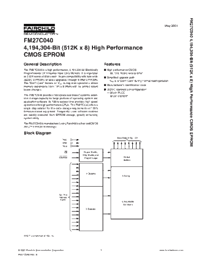
                                                                                                                                                      FM27C040 4,194,304-Bit (512K x 8) High Performance CMOS EPROM
                                                                                                                                   May 2001


     FM27C040
     4,194,304-Bit (512K x 8) High Performance
     CMOS EPROM
     General Description                                                        Features
     The FM27C040 is a high performance, 4,194,304-bit Electrically             I High performance CMOS
     Programmable UV Erasable Read Only Memory. It is organized                   -- 90, 120, 150ns access time*
     as 512K words of 8 bits each. Its pin-compatibility with byte-wide         I Simplified upgrade path
     JEDEC EPROMs enables upgrades through 8 Mbit EPROMs.                         --VPP is a "Don't Care" during normal read operation
     The "Don't Care" feature on VPP during read operations allows
                                                                                I Manufacturer's identification code
     memory expansions from 1M to 8 Mbits with no printed circuit
     board changes.                                                             I JEDEC standard pin configuration
                                                                                  -- 32-pin PLCC
     The FM27C040 provides microprocessor-based systems exten-                    -- 32-pin CERDIP
     sive storage capacity for large portions of operating system and
     application software. Its 120ns access time provides high speed
     operation with high-performance CPUs. The FM27C040 offers a
     single chip solution for the code storage requirements of 100%
     firmware-based equipment. Frequently used software routines
     are quickly executed from EPROM storage, greatly enhancing
     system utility.
     The FM27C040 is manufactured using Fairchild's advanced CMOS
     AMGTM EPROM technology.

     Block Diagram
                                                                                           Data Outputs O0 - O7
                                            VCC
                                            GND
                                            VPP


                                              OE          Output Enable,
                                                         Chip Enable, and
                                         CE/PGM                                                  Output
                                                          Program Logic
                                                                                                 Buffers


                                                            Y Decoder
                                                                                ..


                                                                                               Y Gating


                                         A0 - A18
                                         Address
                                          Inputs
                                                                                .......


                                                                                               4,194,304-Bit
                                                                                                Cell Matrix
                                                            X Decoder


     AMGTM is a trademark of WSI, Inc.
◦ Jabse Service Manual Search 2026 ◦ Jabse Pravopis ◦ onTap.bg ◦ Other service manual resources online : Fixya ◦ eServiceinfo