Service Manuals, User Guides, Schematic Diagrams or docs for : . Electronic Components Datasheets Various datasheets 74ls109

<< Back | Home

Most service manuals and schematics are PDF files, so You will need Adobre Acrobat Reader to view : Acrobat Download Some of the files are DjVu format. Readers and resources available here : DjVu Resources
For the compressed files, most common are zip and rar. Please, extract files with Your favorite compression software ( WinZip, WinRAR ... ) before viewing. If a document has multiple parts, You should download all, before extracting.
Good luck. Repair on Your own risk. Make sure You know what You are doing.


Image preview - the first page of the document
74ls109


>> Download 74ls109 documenatation <<

Text preview - extract from the document
                                                                                                     SN54/74LS109A
DUAL JK POSITIVE
EDGE-TRIGGERED FLIP-FLOP
   The SN54 / 74LS109A consists of two high speed completely independent
transition clocked JK flip-flops. The clocking operation is independent of rise
and fall times of the clock waveform. The JK design allows operation as a D                              DUAL JK POSITIVE
flip-flop by simply connecting the J and K pins together.                                            EDGE-TRIGGERED FLIP-FLOP
                                                                                                          LOW POWER SCHOTTKY
                                        LOGIC DIAGRAM


           SET (SD)
             5(11)
                                                                                               Q
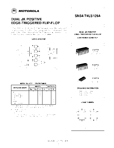
        CLEAR (CD)                                                                           6(10)                                  J SUFFIX
           1(15)                                                                                                                    CERAMIC
            CLOCK                                                                                                                  CASE 620-09
             4(12)                                                                                   16
                                                                                                          1
                                                                                              Q
                                                                                             7(9)
                 J
               2(14)

                 K                                                                                                                  N SUFFIX
               3(13)                                                                                                                PLASTIC
                                                                                                     16                            CASE 648-08
                                                                                                          1


                                                                                                                                     D SUFFIX
                                                                                                                                       SOIC
                                                                                                          16
                                                                                                                1                  CASE 751B-03
                 MODE SELECT -- TRUTH TABLE
                                             INPUTS                 OUTPUTS
   OPERATING MODE                                                                                         ORDERING INFORMATION
                                   SD       CD       J       K        Q       Q
                                                                                                           SN54LSXXXJ            Ceramic
  Set                               L        H       X       X        H       L
                                                                                                           SN74LSXXXN            Plastic
  Reset (Clear)                     H        L       X       X        L       H
                                                                                                           SN74LSXXXD            SOIC
  *Undetermined                     L        L       X       X        H       H
  Load "1" (Set)                    H        H       h       h        H       L
  Hold                              H        H       l       h        q       q
  Toggle                            H        H       h       l        q       q
  Load "0" (Reset)                  H        H       l       l        L       H                                     LOGIC SYMBOL
* Both outputs will be HIGH while both SD and CD are LOW, but the output states
  are unpredictable if SD and CD go HIGH simultaneously.                                                            5                   11
H, h = HIGH Voltage Level
L, I = LOW Voltage Level                                                                                       J SD Q       6 14 J SD
                                                                                                      2                               Q        10
X = Don't Care
l, h (q) = Lower case letters indicate the state of the referenced input (or output)                           CP              12 CP
                                                                                                      4
l, h (q) = one set-up time prior to the LOW to HIGH clock transition.
                                                                                                                            7 13
                                                                                                      3        K C Q                   K C Q   9
                                                                                                                  D                       D

                                                                                                                    1                   15

                                                                                                                        VCC = PIN 16
                                                                                                                        GND = PIN 8


                                                                    FAST AND LS TTL DATA
                                                                                       5-1
                                                               SN54/74LS109A

GUARANTEED OPERATING RANGES
  Symbol                                   Parameter                                                    Min         Typ           Max             Unit
  VCC            Supply Voltage                                                             54          4.5          5.0          5.5              V
                                                                                            74          4.75         5.0          5.25
  TA             Operating Ambient Temperature Range                                        54          


◦ Jabse Service Manual Search 2024 ◦ Jabse PravopisonTap.bg ◦ Other service manual resources online : FixyaeServiceinfo